Deformable mirror and optical controller including the deformable mirror

a technology of optical controller and deformation mirror, which is applied in the direction of optics, optical elements, instruments, etc., can solve the problems of reducing the response speed of continuous mirror, unable to obtain electrostatic force, and difficulty in ensuring the control range of continuous mirror and reducing the drive voltag

Inactive Publication Date: 2006-06-27
PANASONIC CORP
View PDF24 Cites 38 Cited by
  • Summary
  • Abstract
  • Description
  • Claims
  • Application Information

AI Technical Summary

Benefits of technology

[0017]A deformable mirror according to the present invention includes: a substrate; a plurality of micromirrors, which are supported by the substrate while being segmented from each other; and a plurality of driving sections, which drive the micromirrors independently of each other, thereby controlling arrangements of the respective micromirrors with respect to the substrate. Each of the driving sections includes: a number of fixed electrodes, to which drive voltages are applicable independently of each other; and the same number of movable electrodes, which are provided so as to face the fixed electrodes. Each of the micromirrors is coupled to at least two of the movable electrodes, which are associated with the micromirror. The deformable mirror can displace each micromirror perpendicularly to the substrate and / or tilt the micromirror with respect to the substrate by utilizing an electrostatic force to be produced due to a potential difference between the at least two movable electrodes and at least two of the fixed electrodes that are associated with the movable electrodes.
[0022]In another preferred embodiment, either the first conductive portion or the second conductive portion and the intermediate coupling member are rotatable freely by way of the protrusion members.

Problems solved by technology

However, in utilizing an electrostatic force, basically only the attraction works unlike the case of using a piezoelectric element.
Nevertheless, it is difficult for the continuous mirror to secure a control range and reduce the drive voltage at the same time.
Thus, no electrostatic force can be obtained unless a high voltage is applied.
In addition, the continuous mirror has a lower response speed than the segmented mirror, and the residual stress of the mirror film seriously affects the planarity of the mirror.
However, the conventional segmented mirror attracts and shifts the respective mirrors parallel and can produce only a stepped wavefront.
As a result, the control structure gets too much complicated or the area of the gap between the mirrors increases with respect to the area of each mirror.
Consequently, the reflection efficiency decreases and the effects of unwanted diffracted light increase.
But this segmented mirror has no compatibility with a semiconductor device manufacturing process and is hard to mass-produce at a low cost.
Firstly, it is difficult for the electrostatic deformable mirror, producing only the attraction, to control the parallel shifting operation and the tilting operation independently.
Secondly, unlike the piezoelectric element that generates a driving force by its own structural expansion or shrinkage, the electrostatic deformable mirror needs a pair of electrodes, which is arranged with a gap provided between them, and a structure for supporting the electrodes as separate members. Thus, it is difficult to provide the pair of electrodes, of which the area is broad enough to obtain a big electrostatic force, and the supporting structure, which enables both the parallel shifting operation and tilting operation alike, within the limited areas of segmented mirrors of such a deformable mirror.

Method used


Image

  • Deformable mirror and optical controller including the deformable mirror
  • Deformable mirror and optical controller including the deformable mirror
  • Deformable mirror and optical controller including the deformable mirror

Examples


embodiment 1

[0037]First, a deformable mirror according to a first preferred embodiment of the present invention will be described with reference to FIGS. 1 and 2.

[0038]The deformable mirror of this preferred embodiment has a configuration in which a plurality of actuators (i.e., driving sections) and a driver circuit for driving those actuators are integrated together on the same silicon substrate. This deformable mirror is preferably fabricated by semiconductor processing technologies.

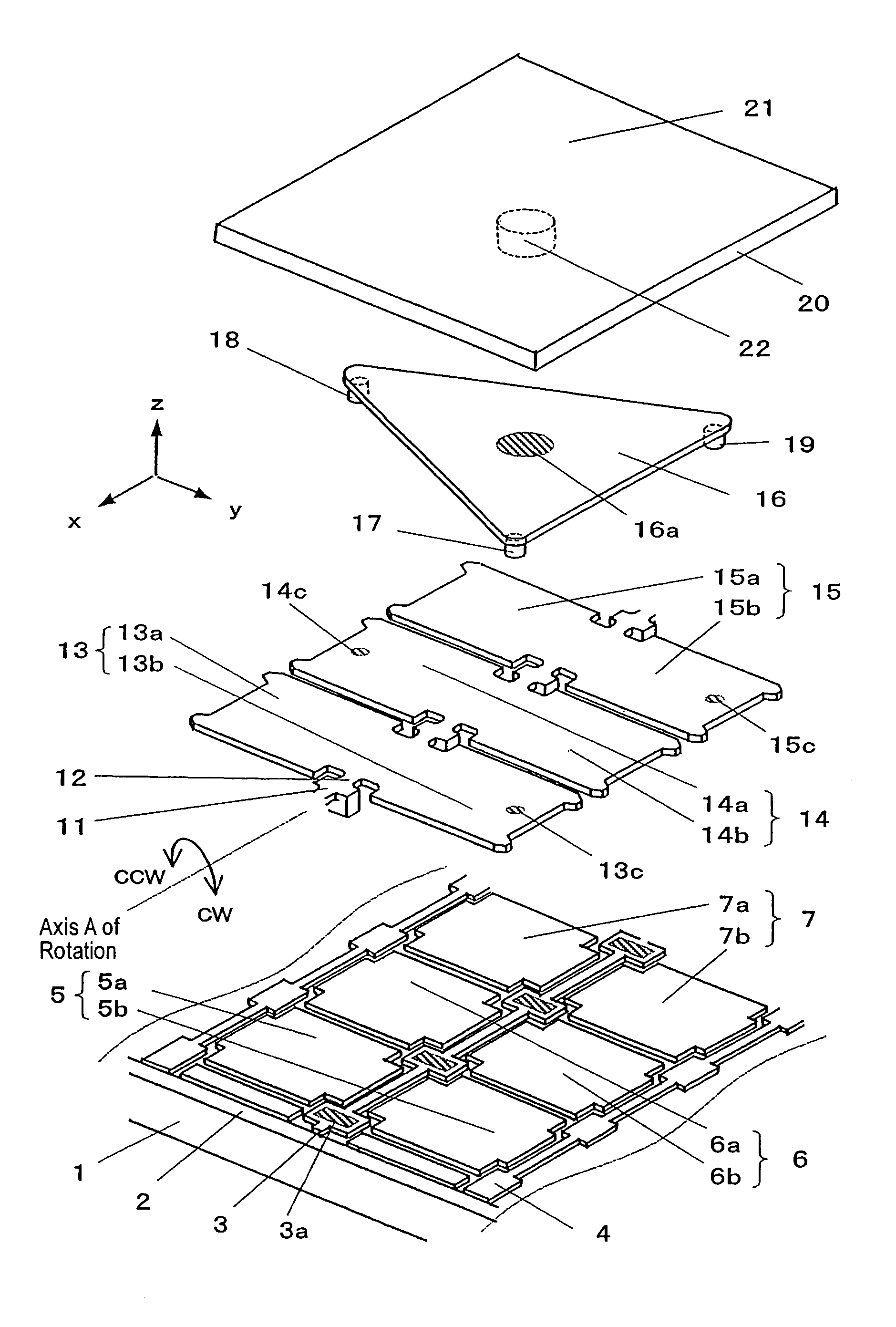
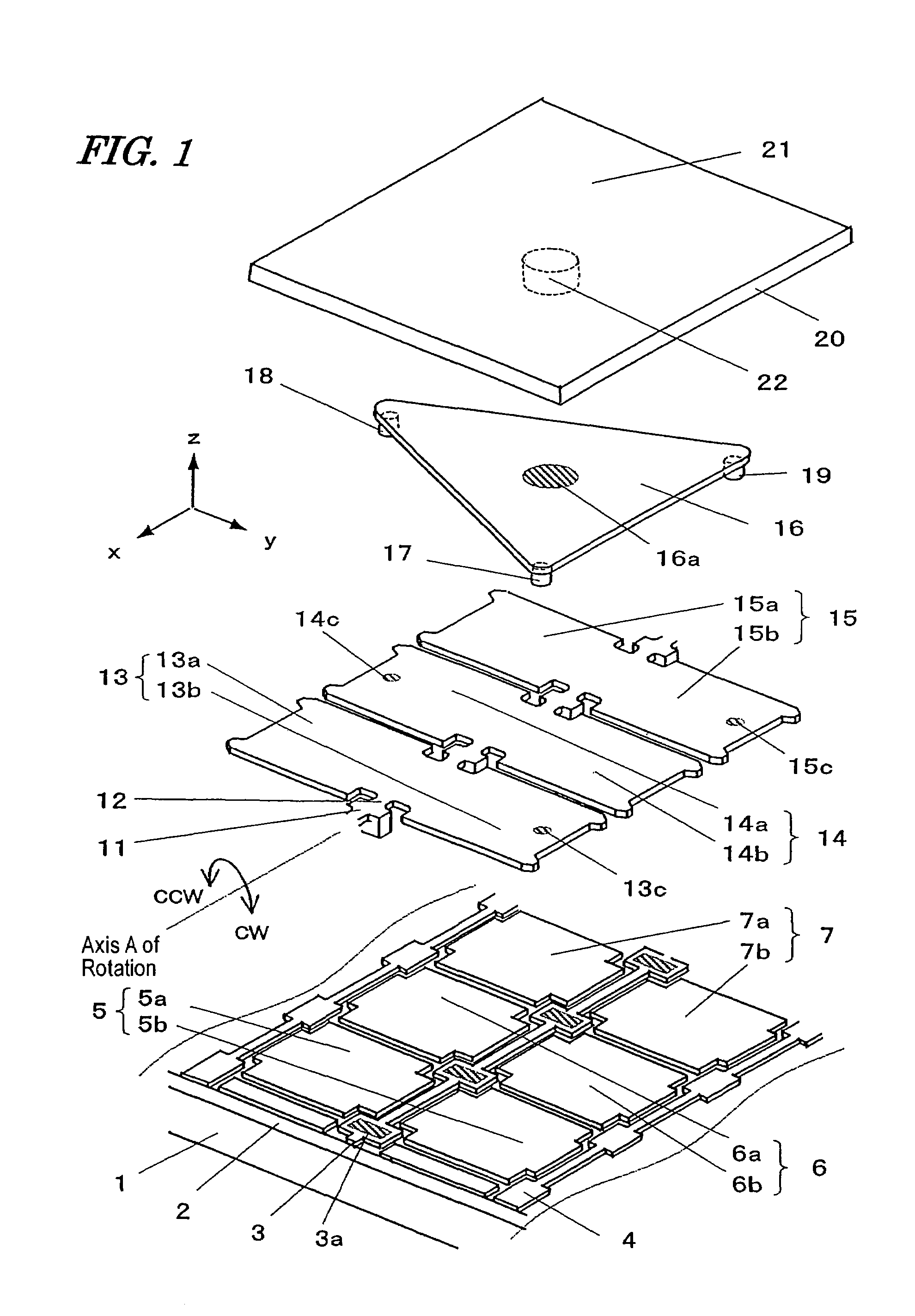
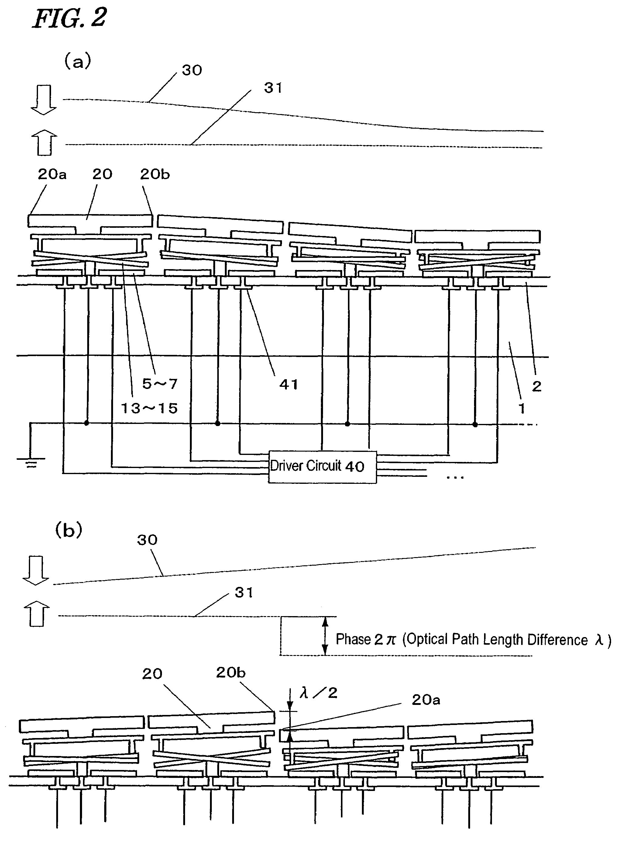
[0039]Referring to FIG. 1, illustrated is an exploded perspective view of a deformable mirror according to this preferred embodiment. The deformable mirror of this preferred embodiment actually has a configuration in which a plurality of micromirrors (or reflective mirror elements) 20 are arranged in a two-dimensional array. In FIG. 1, just one of those micromirrors 20 and its associated driving section are illustrated on a large scale.

[0040]In the deformable mirror of this preferred embodiment, the driving secti...

embodiment 2

[0070]Hereinafter, a deformable mirror according to a second preferred embodiment of the present invention will be described with reference to FIG. 3. FIG. 3 is an exploded perspective view of a deformable mirror according to this preferred embodiment.

[0071]The difference between the deformable mirror of this preferred embodiment and the counterpart of the first preferred embodiment lies in the configuration of the intermediate coupling member 50. That is to say, the deformable mirrors of this and first preferred embodiments have the same configuration as for the substrate 1, insulating layer 2, base 3, yoke contact portion 4, fixed electrodes 5 to 7, supporting post 11, hinge 12, yokes 13 to 15, protrusion members 17 to 19, micromirror 20, reflective plane 21 and protrusion 22.

[0072]The intermediate coupling member 50 of this preferred embodiment includes three pairs of hinge portions 50b. Each hinge portion 50b supports its associated protrusion member 17, 18 or 19 in a freely rot...

embodiment 3

[0074]Hereinafter, a deformable mirror according to a third preferred embodiment of the present invention will be described with reference to FIG. 4. FIG. 4 is an exploded perspective view of a deformable mirror according to this preferred embodiment.

[0075]The deformable mirror of this preferred embodiment is different from the counterpart of the second preferred embodiment in the configuration of fixed electrodes 60, 61 and 62. More specifically, the first fixed electrode 60 of this preferred embodiment is divided into fixed-electrode pieces 60a and 60b, and each of the fixed-electrode pieces 60a and 60b is further subdivided into eight partial electrodes, to which drive voltages are applicable independently of each other. The following description will be focused on the fixed-electrode piece 60a, but the same statement is applicable to the other fixed-electrode piece 60b of the first fixed electrode 60 and to the fixed-electrode pieces 61a, 61b, 62a and 62b of the second and third...


PUM


Abstract

A deformable mirror according to the present invention includes a substrate 1, a plurality of micromirrors 20, which are supported by the substrate 1 while being segmented from each other, and a plurality of driving sections, which drive the micromirrors 20 independently of each other. Each of the driving sections includes a number of fixed electrodes 5 to 7, and the same number of movable electrodes 13 to 15, which are provided so as to face the fixed electrodes 5 to 7. Each of the micromirrors 20 is coupled to at least two of the movable electrodes 13 to 15, which are associated with the micromirror 20. The deformable mirror can displace each micromirror 20 perpendicularly to the substrate 1 and / or tilt the micromirror 20 with respect to the substrate.

Description

CROSS-REFERENCE TO RELATED APPLICATION[0001]This application is a Section 371 of International Application No. PCT / JP02-12344, filed Nov. 26, 2002, the disclosure of which is incorporated herein by reference.TECHNICAL FIELD[0002]The present invention relates to a deformable mirror having a light reflecting region that can displace with an electrostatic force and also relates to an optical controller for controlling the wavefront of light with such a deformable mirror.BACKGROUND ART[0003]Deformable mirrors are going to find applications in optical compensators for correcting the wave aberration of light actively, displays, and optical switches for use in optical communication. Recently, there are a number of R & D reports that a bunch of micromirrors be formed by a micro-machining technique to cut down the cost. Those micromirrors are often driven with an electrostatic force. A type of deformable mirror, driving the micromirrors with an electrostatic force, has a planar and simple st...

Claims


Application Information

Patent Timeline
Patent Type & Authority Patents(United States)
IPC IPC(8): G02B26/00G02B26/08
CPCG02B26/0841Y10S359/904G02B26/06G02B26/08
Inventor MUSHIKA, YOSHIHIRO
Owner PANASONIC CORP
Why Eureka
Try Eureka