
Method for manufacturing image display device
a technology of image display device and manufacturing method, which is applied in the manufacture of electric discharge tube/lamp, discharge tube luminescnet screen, discharge tube/lamp, etc., can solve the problems of preventing stable production of high-quality image display device, affecting the display image, and not ensuring the assembly position of the spacer
- Summary
- Abstract
- Description
- Claims
- Application Information
AI Technical Summary
Benefits of technology
Problems solved by technology
Method used
Image

Examples
examples
[0122]While examples of the present invention will be described hereinafter, it is to be understood that the invention is not limited to those.
first example
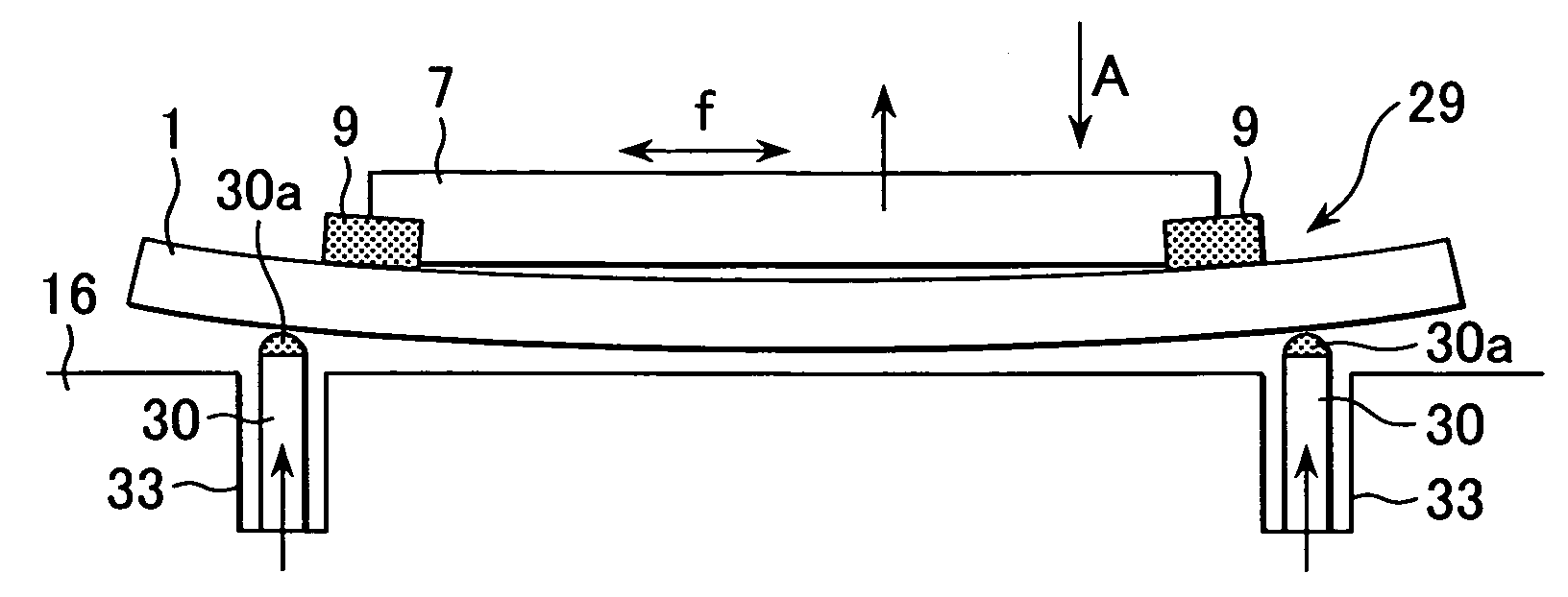
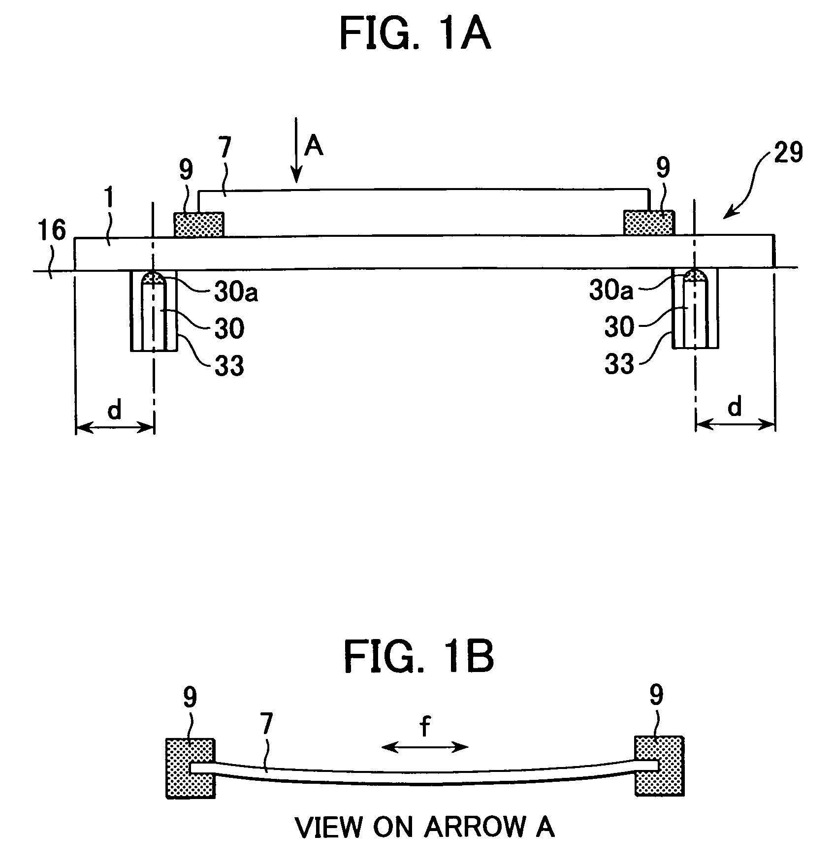
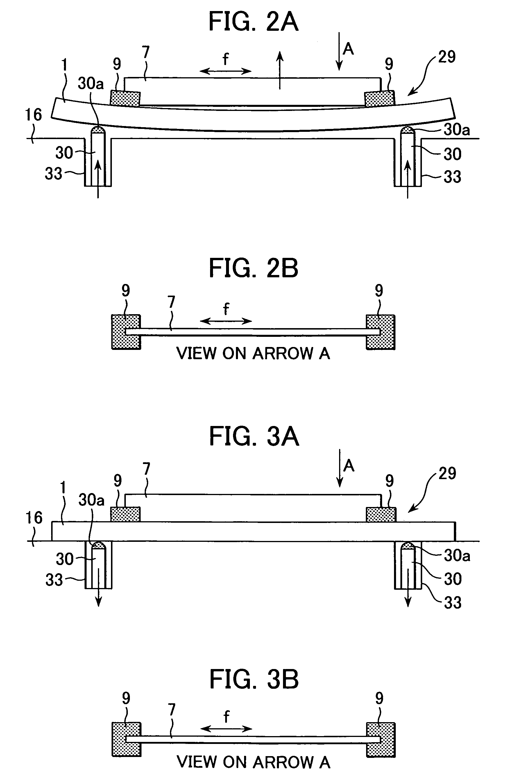
[0123]In this example, a first substrate (rear plate) with a spacer is deformed to thereby form a space between the spacer and the surface of the rear plate, correcting the position of the spacer by the space, and thus realizing a correct arrangement relationship.
[0124]FIG. 1A to FIG. 3B are schematic diagrams for explaining the process of forming a space between the plate spacer 7 and the surface of the rear plate 1 in this example. The example will be described with reference to FIGS. 1A to 3B.
[0125]A plurality of the plate spacers 7 is bonded and fixed onto the rear plate 1 at regular spaces with tension loaded along the length of the spacer 7.
[0126]When an external impact and so on are applied to the rear plate 1 having the plate spacer 7 due to transfer or the like after the completion of assembly of the plate spacer 7 and the rear plate 1 until the start of assembly of the rear plate 1 and the face plate 3, as described above, the center of the plate spacer 7 may sometimes dev...
second example
[0137]In this example, the support member on opposite ends of the spacer was made of a member that is deformed by heat, allowing the formation of a space between the spacer and the rear plate under high temperature, correcting the position of the spacer by the space, and thus realizing an accurate arranging relationship.
[0138]The characteristics of this example for making the image display device having the structure shown in FIGS. 29 and 30 will be described hereinafter.
(Plate Spacer)
[0139]The plate spacer 1020 (refer to FIG. 30) was made of a soda-lime-glass insulating member (300 mm×2 mm×0.2 mm).
[0140]The high-resistance layer 1021 was formed on four faces exposed in the image forming region of the airtight container of the surfaces of the spacer 1020 (the front and back faces of 300 mm×2 mm and 300 mm×0.2 mm, respectively, or the faces exposed in vacuum), while the low-resistance layer 1022 was formed on two faces 1023 in contact with the respective image forming regions of the ...
PUM
| Property | Measurement | Unit |
|---|---|---|
| temperature | aaaaa | aaaaa |
| temperature | aaaaa | aaaaa |
| thickness | aaaaa | aaaaa |
Abstract
Description
Claims
Application Information