Liquid crystal display device

Inactive Publication Date: 2008-10-23
NEC LCD TECH CORP
View PDF16 Cites 14 Cited by
  • Summary
  • Abstract
  • Description
  • Claims
  • Application Information

AI Technical Summary

Benefits of technology

[0026]An object of the present invention is to provide a LCD device that makes it possible to prevent the gray level folding in at least one of the vicinity of the highest gray level and that of the lowest gray level while avoi

Problems solved by technology

Accordingly, a problem of “gray level folding” occurs in the intermediate tones in the vicinities of white and black.
However, the above-described LCD device of the prior art 1 has the problem that the

Method used


Image

  • Liquid crystal display device
  • Liquid crystal display device
  • Liquid crystal display device

Examples


Example

First Embodiment

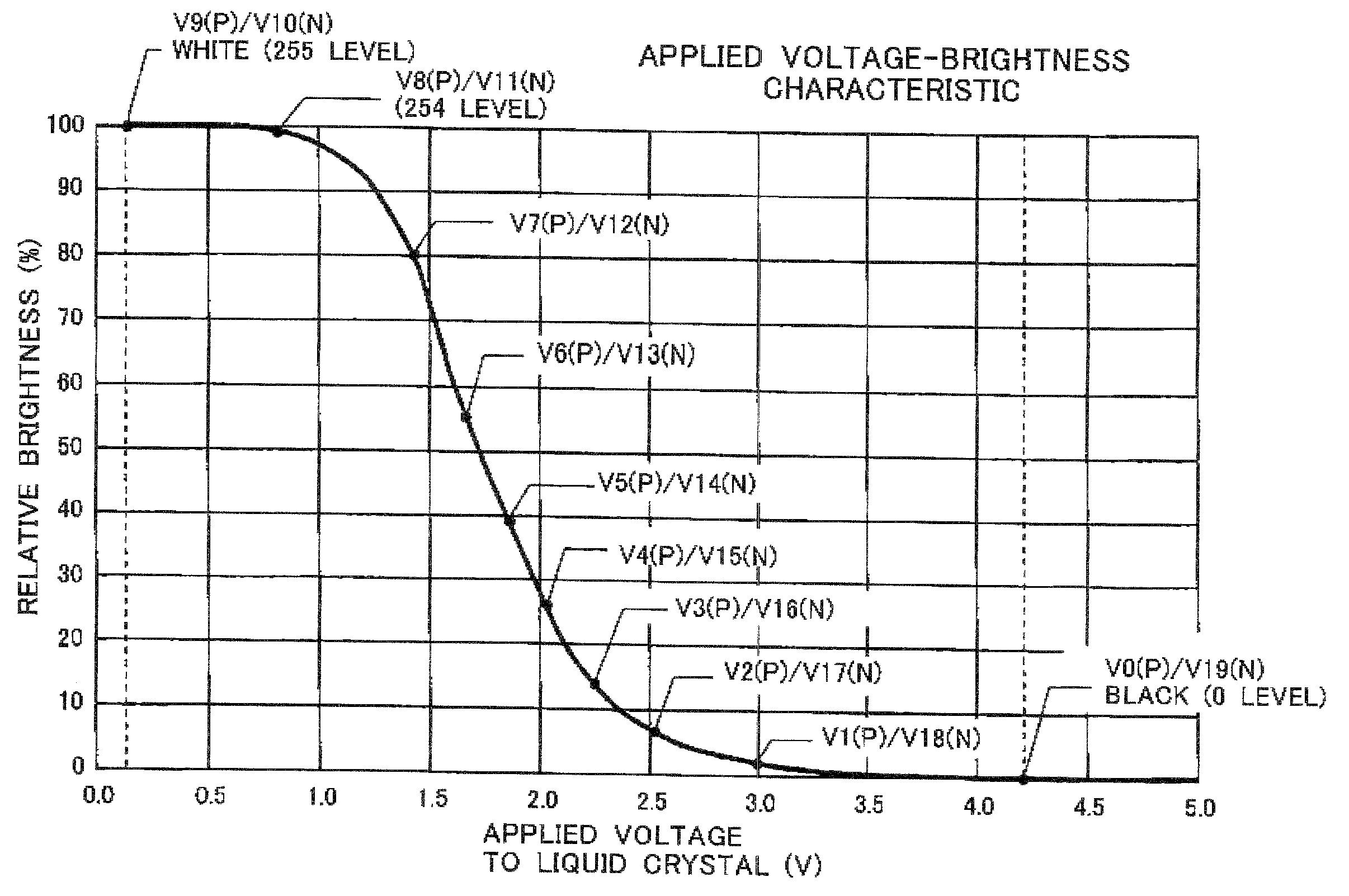
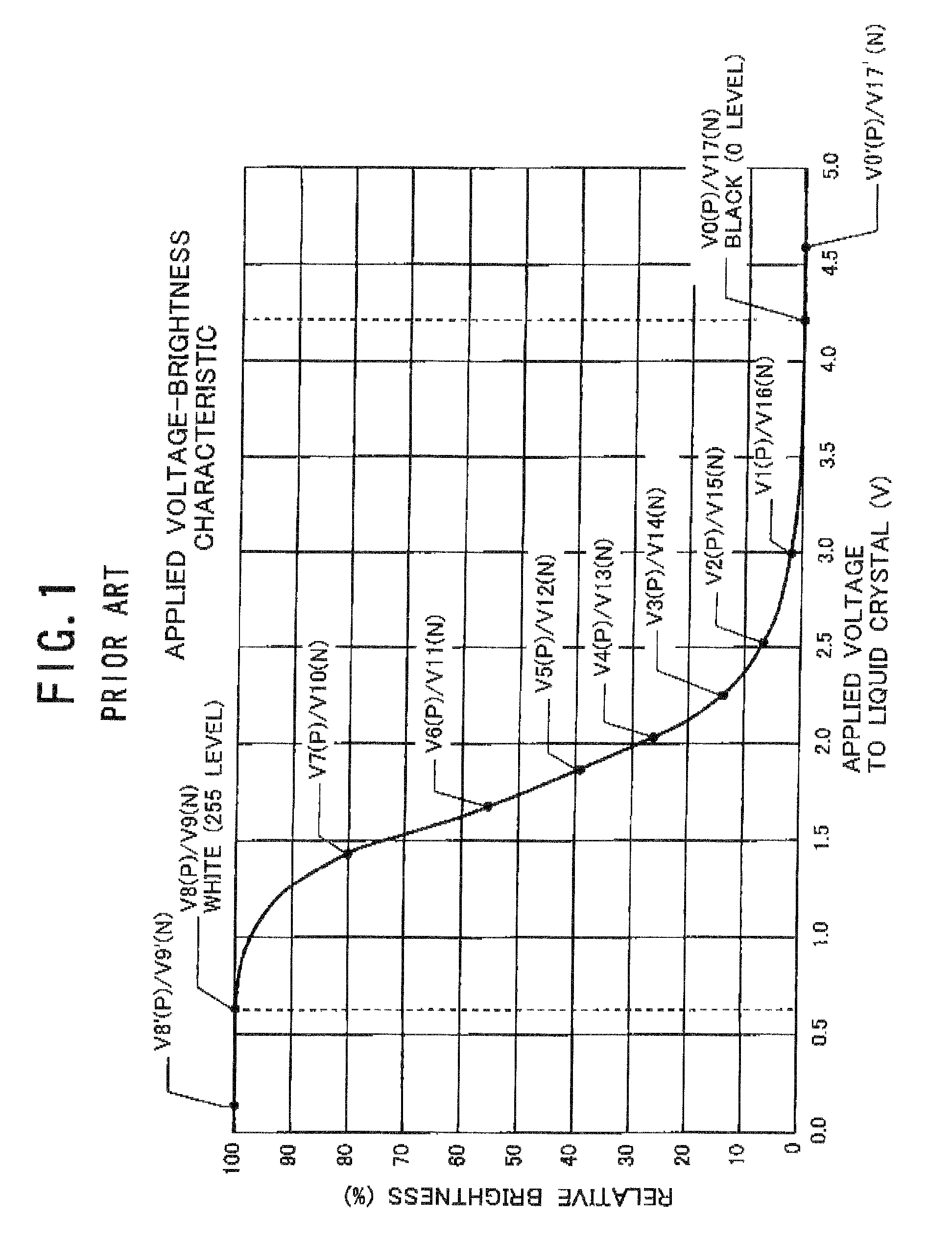
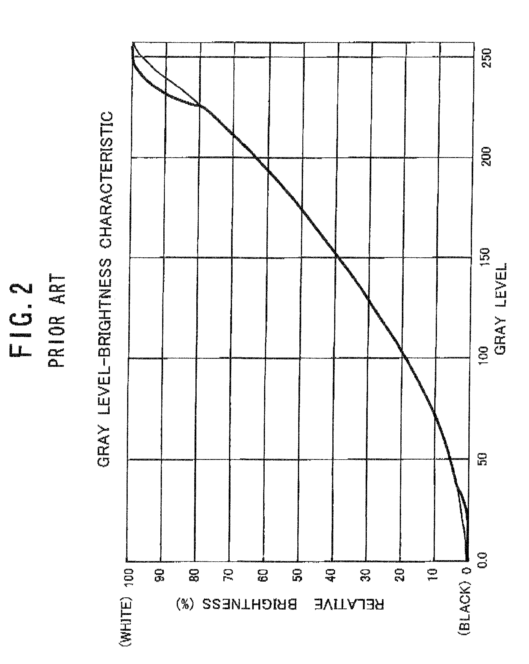
[0094]The applied voltage-brightness characteristic of an active-matrix addressing LCD device according to a first embodiment of the invention is shown in FIG. 6, which operates in the normally white and TN mode. The gray level-brightness characteristic used in this LCD device is shown in FIG. 7. This device displays images with 8 bits on a 256-level gray scale from a 0 level as the lowest level to a (255−1) level as the highest level. Therefore, the gray level number M is 256.

[0095]The LCD device according to the first embodiment comprises a LCD panel 10 as the display section, as shown in FIG. 14. The LCD panel 10 has a plurality of pixels arranged in a matrix array. These pixels are defined by scanning lines 13 and data lines (or signal lines) 14 that are arranged on the panel 10 in such a way as to be intersected at right angles. A TFT 15 as a switching element for driving the pixel and a pixel electrode 16 are provided for each of the pixels. The scanning lines ...

Example

Second Embodiment

[0120]FIG. 10 schematically shows the front view an active-matrix addressing LCD device according to a second embodiment of the present invention, where the display screen of the said device is viewed from the CF substrate side. This device operates in the normally white and TN mode similar to the above-described first embodiment.

[0121]Generally, an active-matrix addressing LCD device is constituted by coupling a CF substrate and a TFT substrate. In the TN mode, the alignment directions of the liquid crystal molecules on the CF and TFT substrates are regulated by the alignment films formed respectively on these two substrates. Therefore, the liquid crystal molecules are aligned along the rubbing directions of the CF and TFT substrates. Accordingly, the liquid crystal molecules have pretilt angles in the range of 2° to 10° on the surfaces of the CF and TFT substrates. A chiral agent is added to the liquid crystal to twist the liquid crystal molecules along a single d...

Example

Third Embodiment

[0146]FIG. 13 shows the applied voltage-brightness characteristic of the LCD device according to a third embodiment of the invention, which is viewed from the front of the said device. This device operates in the normally white and TN mode similar to the above-described first embodiment.

[0147]To display images with 8 bits at 256 gray levels as shown in FIG. 7, reference voltages having 22 levels including the positive and negative polarities (i.e., V0 to V21 in the applied voltage-brightness characteristic of FIG. 13) are applied to the data line driver circuit 12. The data line driver circuit 12 divides each of the spaces among the reference voltages V0 to V21 based on the said reference voltages by a predetermined procedure, thereby generating the output voltages having 256 levels including the positive and negative polarities. Thereafter, one of the 256 output voltages corresponding to the inputted image data is selected for each data line 14, and the selected out...


PUM


Abstract

A liquid crystal display device prevents the gray level folding in at least one of the vicinities of the highest and lowest gray levels while avoiding the complication of the data line driver circuit. The data line driver circuit generates output voltages whose number is equal to a predetermined gray level number M based on reference voltages, and selects one of the output voltages and outputs the selected one to the display section in response to an inputted image signal, thereby displaying images The applied voltage-brightness characteristic of the display section has a zero brightness change region in which the reference voltage corresponding to the highest gray level is located. The reference voltage corresponding to the next lower level to the highest level is set such that the brightness at the next lower level is lower than that at the highest level by a predetermined difference.

Description

BACKGROUND OF THE INVENTION[0001]1. Field of the Invention[0002]The present invention relates to a Liquid Crystal Display (LCD) device and more particularly, to a LCD device that improves the time-varying or moving image displaying performance in the Twisted Nematic (TN) mode.[0003]2. Description of the Related Art[0004]The LCD device comprises a transparent substrate on which switching elements such as Thin-Film Transistors (TFTs) are formed (which is usually termed the “TFT substrate” or “driver substrate”), another transparent substrate on which a color filter and a black matrix are formed (which is usually termed the “color filter (CF) substrate” or “opposite substrate”), and a liquid crystal layer sandwiched between the TFT substrate and the CF substrate. An electric field is applied across the electrodes formed on the TFT substrate and those on the CF substrate, or across the electrodes that are formed on the TFT substrate, thereby changing the alignment direction of the liqui...

Claims


Application Information

Patent Timeline
IPC IPC(8): G09G3/36G09G5/10
CPCG09G3/3611G09G2320/0252G09G2320/0261G09G2320/0271G09G2320/0276G09G2320/028G09G2320/066
Inventor INOUE, DAISUKE
Owner NEC LCD TECH CORP
Why Eureka
Try Eureka