Resin-sealed semiconductor device, leadframe with die pads, and manufacturing method for leadframe with die pads
- Summary
- Abstract
- Description
- Claims
- Application Information
AI Technical Summary
Benefits of technology
Problems solved by technology
Method used
Image

Examples
embodiment 1
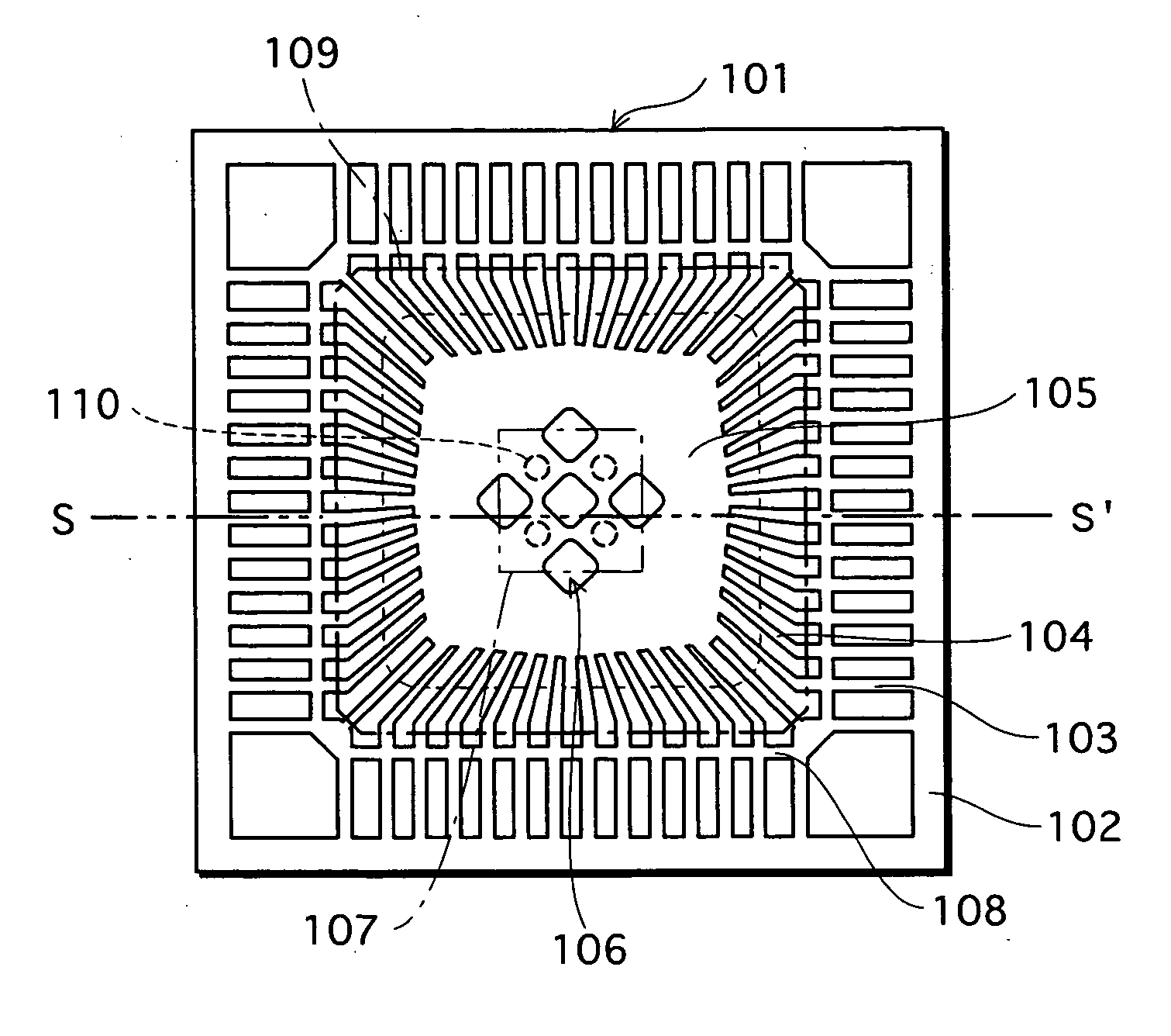
[0045]FIG. 1 is a plan view of an embodiment 1 of a leadframe pertaining to the present invention, while FIG. 2 shows a bottom view of the same.
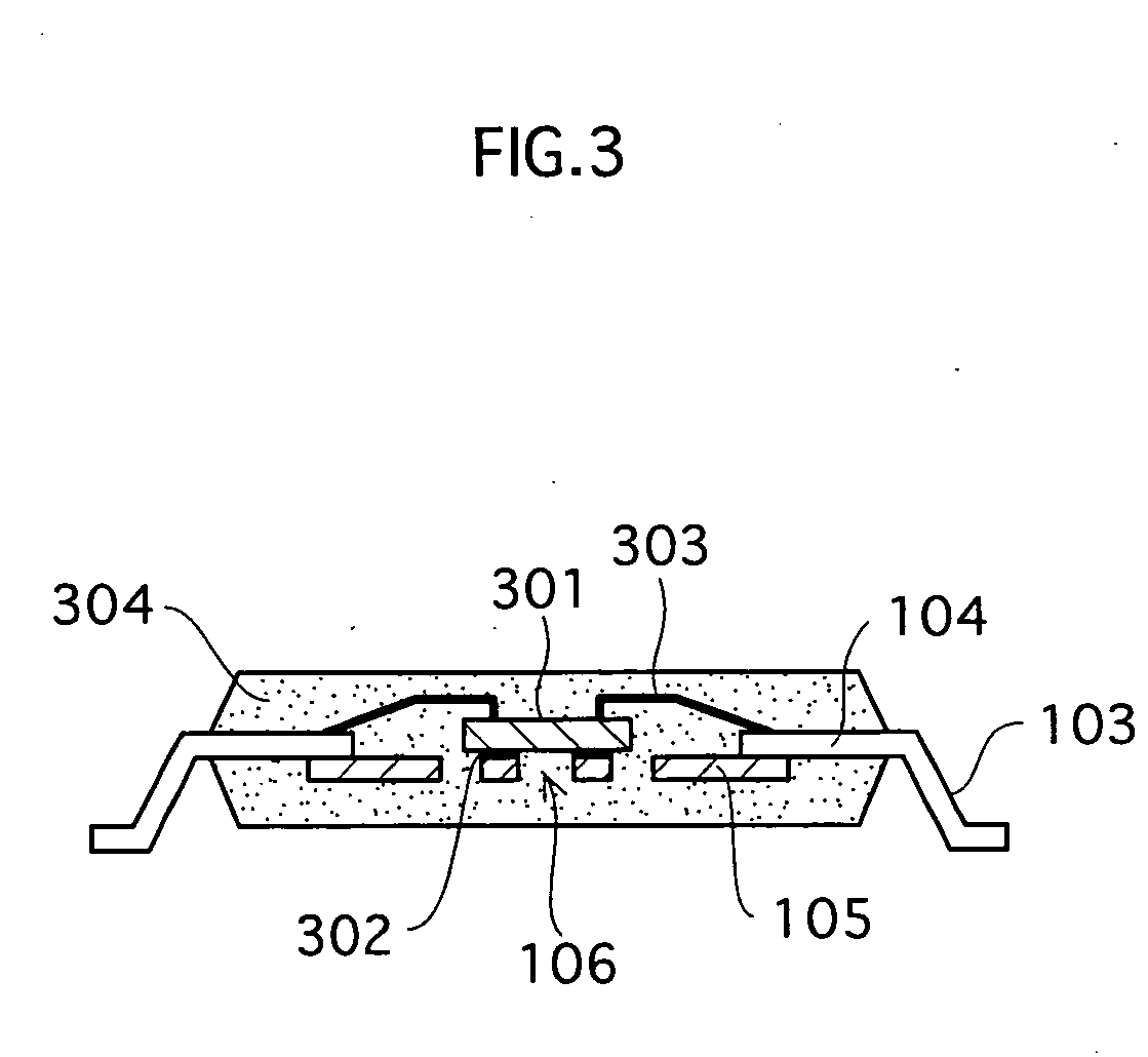
[0046] A leadframe 101 includes a rectangular frame 102, a plurality of outer leads 103 extending at right angles to the four sides of frame 102, a plurality of inner leads 104 that are in series at one end with the outer leads and extend toward the inside of frame 102, and a heat sink 105 adhered to the underside of the opposite ends of inner leads 104. A plurality of substantially square openings 106 with rounded vertices are formed at an approximately 45° angle to the direction in which the outer leads extend. The openings are positioned partially outside a mounting area 107 for the semiconductor element marked by the chain line. The border area between outer leads 103 and inner leads 104 is coupled in the four side directions of frame 102 by a dambar 108. An area 109 marked by the chain line on the inside of dambar 108 indicates the are...
embodiment 2
[0058] An embodiment 2 of a leadframe with die pads and a resin-sealed semiconductor device that uses the leadframe pertaining to the present invention is described next. The following description relates only to the features of the present embodiment, with description of those parts similar to embodiment 1 having been omitted.
[0059]FIG. 5 is a plan view of a leadframe with die pads, while FIG. 6 is a bottom view of the same. A plurality of die pads 502 is provided in mounting area 107 of a leadframe 501 so as to form an oblique checkered-pattern with openings 106. Die pads 502 are substantially square in shape, and as with openings 106 the sides of the die pads are angled at approximately 45 degrees to the direction in which outer leads 103 extend. Those openings 106 positioned circumferentially lie partially outside mounting area 107.
[0060] Since openings 106 and die pads 502 surrounded by openings 106 form a checkered pattern and are angled at approximately 45 degrees to the di...
embodiment 3
[0075] An embodiment 3 of a leadframe with loop-shaped body and a resin-sealed semiconductor device that uses the leadframe pertaining to the present invention is described next. The following description relates only to the features of the present embodiment, with description of those parts similar to embodiment 1 having been omitted.
[0076]FIG. 11 is a plan view of a leadframe with loop-shaped body, while FIG. 12 is a bottom view of the same. Leadframe 1100 consists of the addition of a loop-shaped body 1101 that surrounds mounting area 107 for semiconductor element 301 to leadframe 101 of embodiment 1. Cap-shaped protrusions 1103 that protrude toward semiconductor element 301 are formed centrally on sides of loop-shaped body 1101. Hanging leads 1102 that connect loop-shaped body 1101 to dambar 108 are formed at the corners of loop-shaped body 1101. Note that apart from heat sink 105, leadframe 1100 is integrally formed from sheet metal.
[0077]FIG. 13 is a cross-sectional view of ...
PUM
 Abstract
Description
Claims
Application Information
 - R&D
- Intellectual Property
- Life Sciences
- Materials
- Tech Scout
- Unparalleled Data Quality
- Higher Quality Content
- 60% Fewer Hallucinations
Browse by: Latest US Patents, China's latest patents, Technical Efficacy Thesaurus, Application Domain, Technology Topic, Popular Technical Reports.
© 2025 PatSnap. All rights reserved.Legal|Privacy policy|Modern Slavery Act Transparency Statement|Sitemap|About US| Contact US: help@patsnap.com