Electro-optical device and electronic apparatus

a technology of optical devices and electronic devices, applied in semiconductor devices, semiconductor/solid-state device details, instruments, etc., can solve the problems of large leakage or flow of electromagnetic waves from electromagnetic shields

Inactive Publication Date: 2007-02-08
138 EAST LCD ADVANCEMENTS LTD
View PDF1 Cites 13 Cited by
  • Summary
  • Abstract
  • Description
  • Claims
  • Application Information

AI Technical Summary

Benefits of technology

[0008] An advantage of some aspects of the invention is that it provides an electro-optical device which can suppress an influence by noise on image signals and perform high-quality image display, and an electronic apparatus.

Problems solved by technology

However, in such an electro-optical device, with enhancement of high-definition image display and high-frequency image signals, like the technique disclosed in JP-A-2005-77484, even though the electromagnetic shields are formed at the essential places of the driving circuit, a large amount of leakage or flow of electromagnetic waves may occur from the electromagnetic shields, and adjacent signal lines may be capacitively coupled to each other.

Method used


Image

  • Electro-optical device and electronic apparatus
  • Electro-optical device and electronic apparatus
  • Electro-optical device and electronic apparatus

Examples


Embodiment Construction

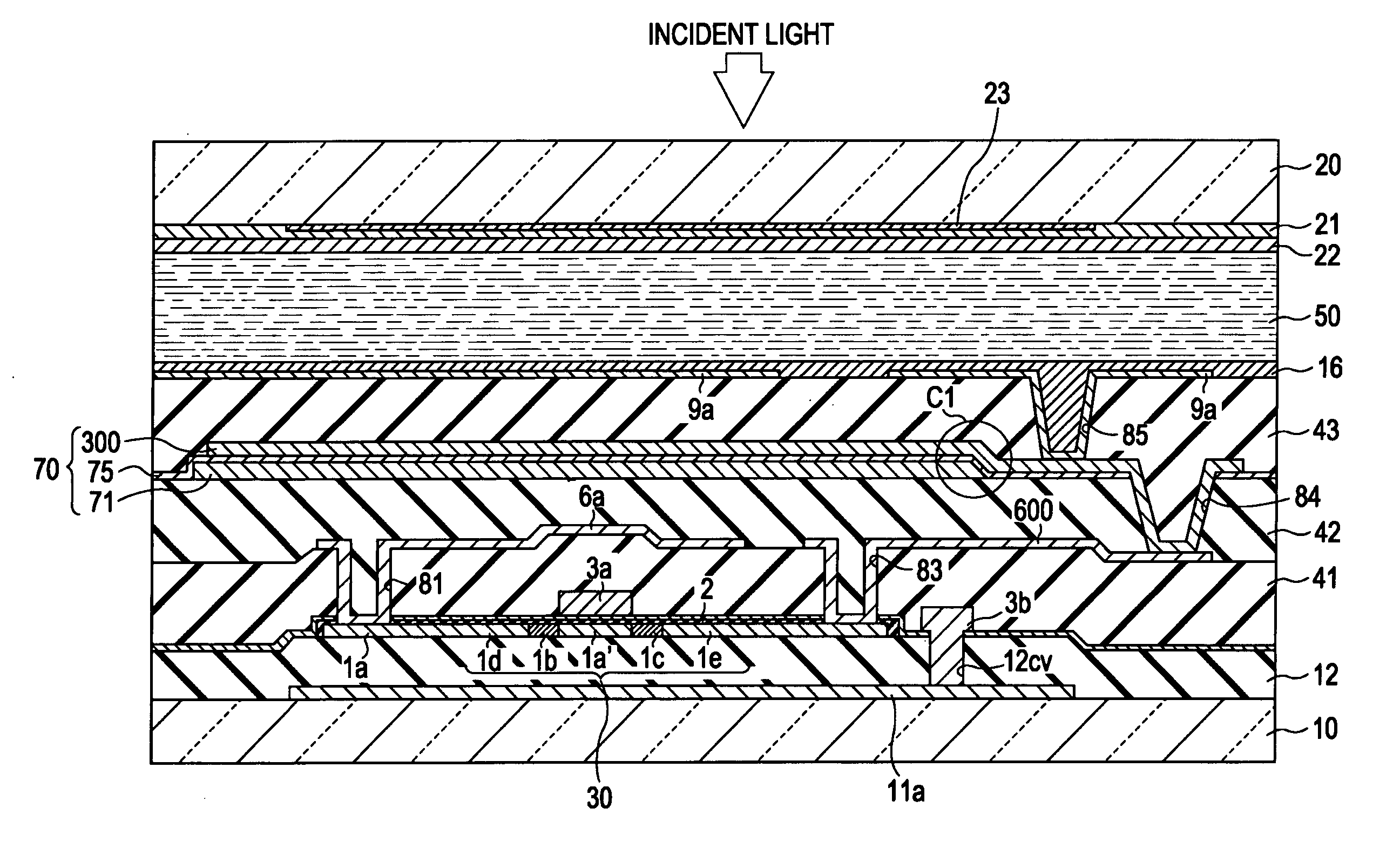
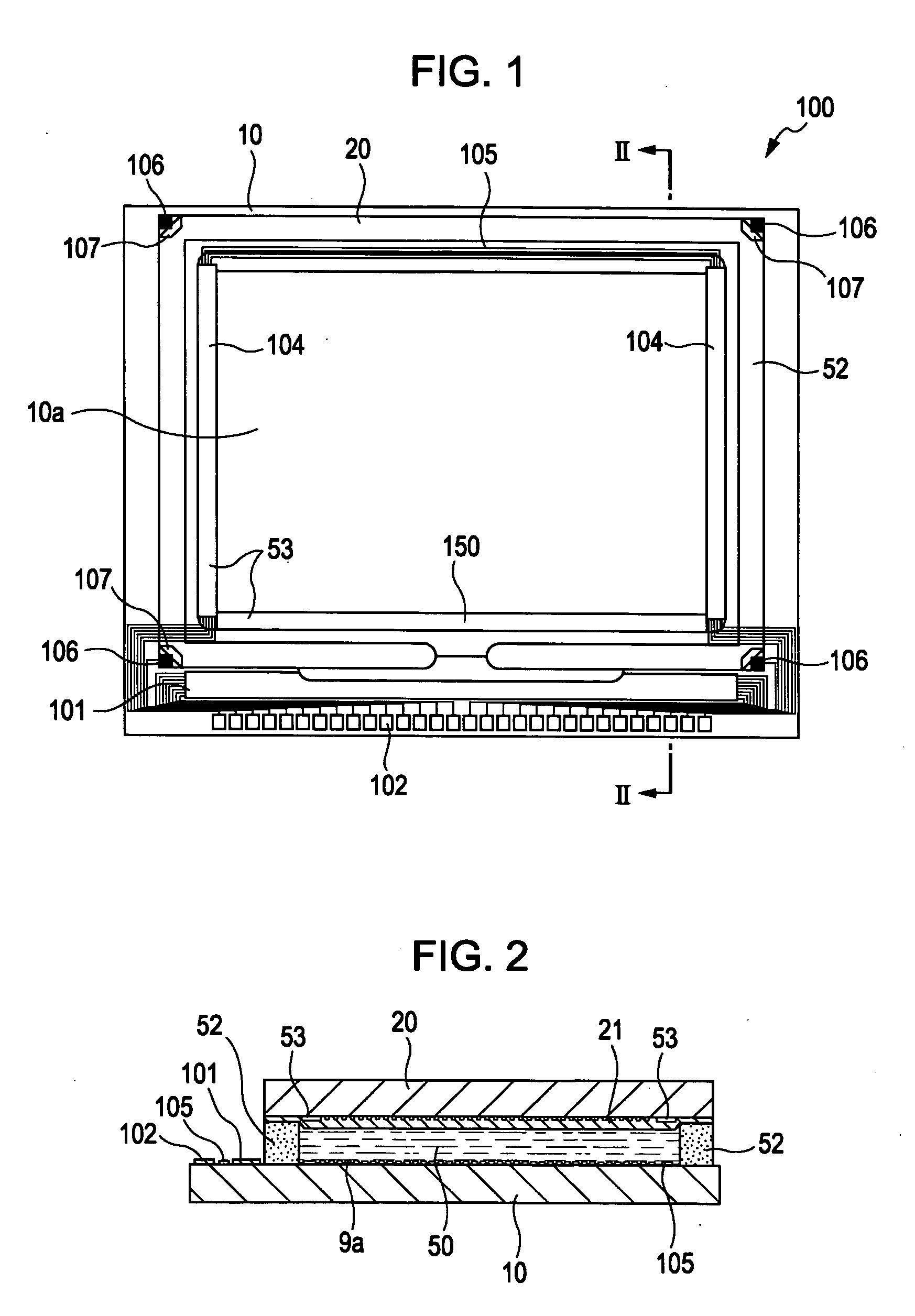
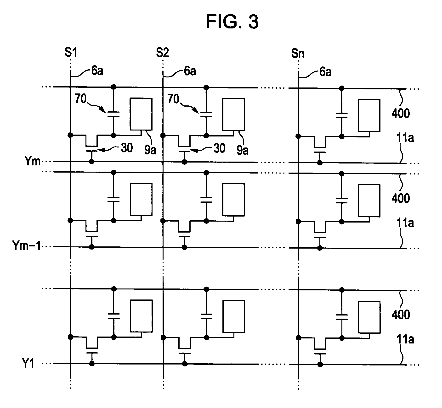
[0044] Hereinafter, an embodiment of the invention will be described with reference to the drawings. FIG. 1 is a plan view showing the configuration of a liquid crystal panel. FIG. 2 is a cross-sectional view taken along the line II-II of FIG. 1. FIG. 3 is an equivalent circuit diagram of various elements, wiring lines, and so on in a plurality of pixels which are formed in a matrix shape so as to form an image display region of a liquid crystal panel. FIGS. 4 to 6 are plan views showing the partial configuration of a pixel portion on a TFT array substrate. FIGS. 4 and 5 correspond to a lower layer portion (FIG. 4) and an upper layer portion (FIG. 5) of a laminated structure described below. FIG. 6 is a plan view showing a laminated structure on a magnified scale, in which FIGS. 4 and 5 are superimposed. FIG. 7 is a cross-sectional view taken along the line VII-VII when FIGS. 4 and 5 are superimposed. FIG. 8 is a block diagram showing the configuration of a liquid crystal device. FI...


PUM


Abstract

An electro-optical device includes first switching elements which are correspondingly provided at intersections of a plurality of scanning lines and a plurality of data lines in a display region, at least three metal layers which are provided in the display region, a wiring line portion which is provided in an adjacent region of the display region and supplies signals to second switching elements through signal lines formed of at least two metal layers of the three metal layers, and an electromagnetic shield which is provided in the adjacent region of the display region. The electromagnetic shield has a first shield portion which covers the wiring line portion using metal layers other than the metal layers forming the signal lines, and a second shield portion which is electrically connected to the first shield portion and is disposed between the signal lines.

Description

BACKGROUND [0001] 1. Technical Field [0002] The present invention relates to an electro-optical device which is suitable for high-definition image display, and to an electronic apparatus. [0003] 2. Related Art [0004] For example, electro-optical devices such as liquid crystal devices have a driving circuit having a data line driving circuit for driving data lines, a scanning line driving circuit for driving scanning lines, and a sampling circuit for sampling image signals. The driving circuit is provided onto a substrate constituting a display unit. In such a driving circuit, at a timing of a sampling circuit driving signal to be supplied from the data line driving circuit, the sampling circuit samples image signals to be supplied onto image signals and supplies the sampled image signals to the data lines. [0005] In an electro-optical device, in order to suppress an increase of a driving frequency and achieve high-definition image display, serial image signals are converted into a p...

Claims


Application Information

Patent Timeline
Patent Type & Authority Applications(United States)
IPC IPC(8): H01L23/552
CPCG02F1/1345G02F2001/133334H01L23/5225H01L23/552H01L2924/0002H01L2924/00G02F1/133334
Inventor NAKAGAWA, MASASHI
Owner 138 EAST LCD ADVANCEMENTS LTD
Why Eureka
Try Eureka