Display apparatus, digital-to-analog conversion circuit and digital-to-analog conversion method

a technology of digital to analog conversion and display apparatus, applied in the direction of code conversion, static indicating devices, instruments, etc., can solve the problems of deterioration in display quality, difficult technical processing of tft with uniform characteristics on glass substrates, and inability to operate at very fast speed, so as to improve display quality

Inactive Publication Date: 2006-11-14
JAPAN DISPLAY CENTRAL CO LTD
View PDF6 Cites 19 Cited by
  • Summary
  • Abstract
  • Description
  • Claims
  • Application Information

AI Technical Summary

Benefits of technology

[0014]It is an object of the present invention to provide a display apparatus capable of improving display quality.
[0015]Moreover, it is another object of the present invention to provide a display apparatus capable of reducing the size of a frame.
[0016]In addition, it is still another object of the present invention to provide a digital-to-analog conversion circuit capable of reducing a time required for digital-to-analog conversion, a display apparatus and a digital-to-analog conversion method.
[0017]Additionally, it is yet another object of the present invention to provide a digital-to-analog conversion circuit which prolongs a period of outputting a result of digital-to-analog conversion by causing a period of performing digital-to-analog conversion processing to partially overlap the period of outputting a result of digital-to-analog conversion, a display apparatus and a digital-to-analog conversion.
[0069]said amplifier having an odd number of inverters which are cascade-connected and maximizing a gain of each inverter in the vicinity of a voltage where the inclination of a voltage-brightness characteristic curve of said display elements becomes maximum.

Problems solved by technology

However, since the operation speed of the TFT formed on the glass substrate is not very fast, various kinds of ingenuity of circuits are required in order to constitute the drive circuit.
Further, forming the TFT with the uniform characteristics on the glass substrate is technically difficult at the present moment, and deterioration in display quality, e.g., irregularities in display may occur due to a difference in characteristics of the TFTs.
Furthermore, when the pixel array portion and the drive circuit are formed on the same glass substrate, a percentage of the pixel array portion which occupies an area of the glass substrate becomes relatively small, and a frame becomes disadvantageously large.
Therefore, the signal line can not possibly satisfactorily rise or fall to a desired voltage, and irregularities in brightness or the like occurs, which leads to degradation in display quality.
Furthermore, the DAC in FIG. 47 and the amplifier provided at the rear stage of the DAC are required for each signal line, and power consumption hence increases and an area occupied by the circuits becomes large, thereby disabling reduction in the frame size.

Method used


Image

  • Display apparatus, digital-to-analog conversion circuit and digital-to-analog conversion method
  • Display apparatus, digital-to-analog conversion circuit and digital-to-analog conversion method
  • Display apparatus, digital-to-analog conversion circuit and digital-to-analog conversion method

Examples


first embodiment

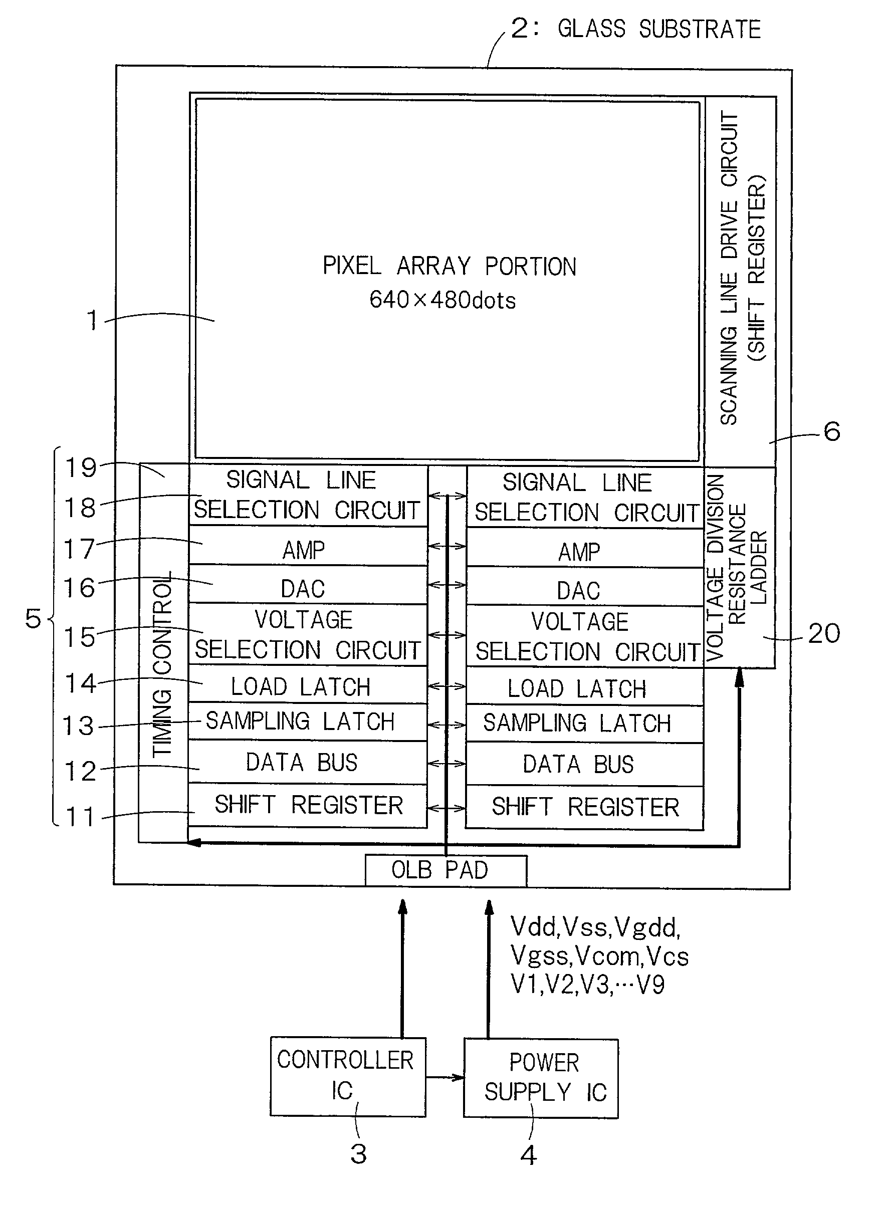
[0192]FIG. 1 is a block diagram showing a schematic structure of a display apparatus according to the present invention and illustrates a block structure of a liquid crystal display apparatus. The liquid crystal display apparatus depicted in FIG. 1 includes a glass substrate 2 in which a pixel array portion 1 and drive circuits are integrally formed. The glass substrate 2 is arranged so as to be opposed to a non-illustrated opposed substrate and sealed with a liquid crystal layer therebetween.

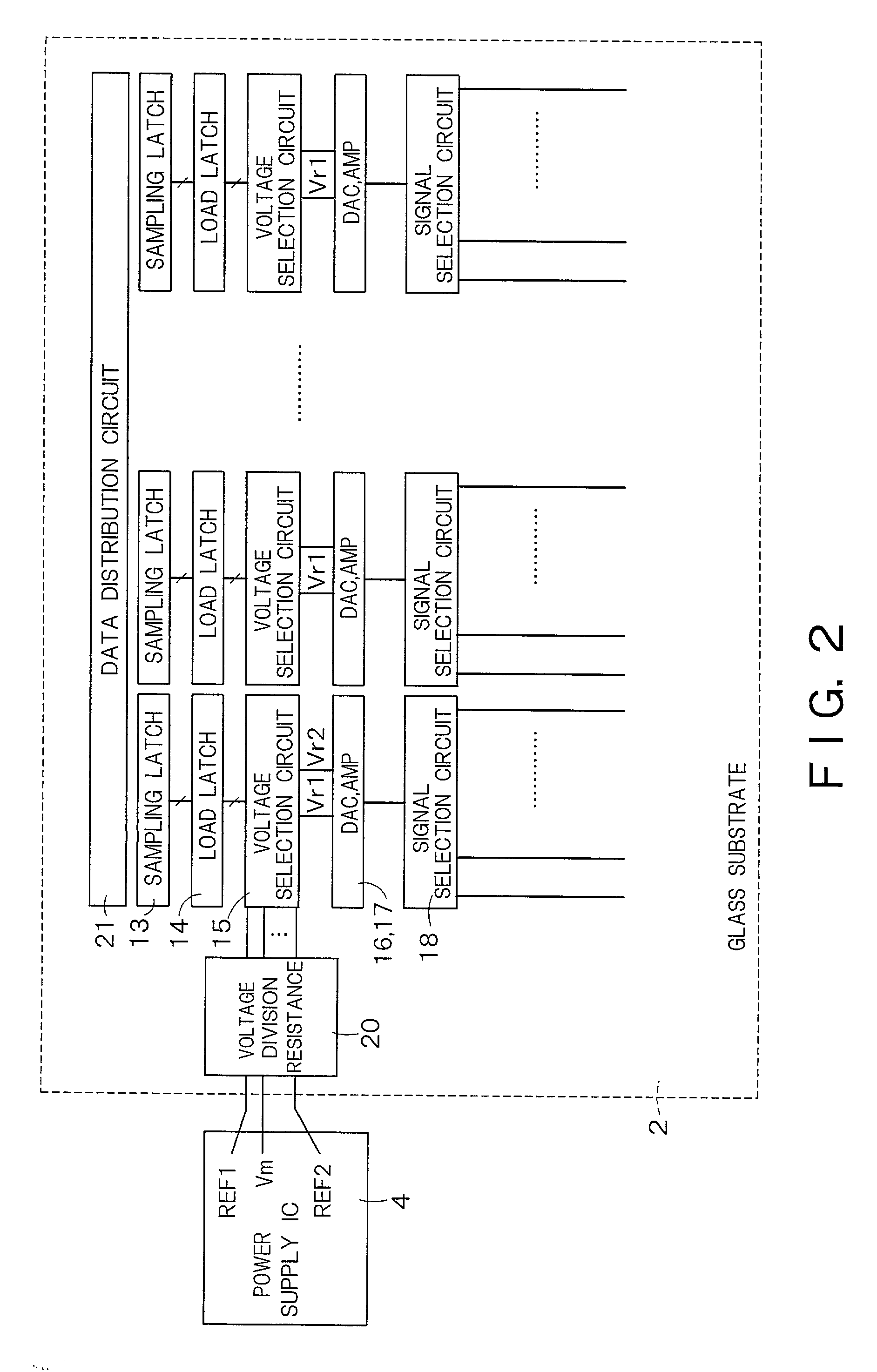
[0193]As separate from the glass substrate 2 illustrated in FIG. 1, there is provided a substrate having mounted thereon a controller IC3 which transmits a digital video signal and a control signal to the drive circuit and a power supply IC4 which supplies a power supply voltage, and these substrates are connected to each other through a flexible printed board or the like.

[0194]On the glass substrate 2 in FIG. 1 are provided the pixel array portion 1 in which signal lines and scanning lines are...

second embodiment

[0214](Second Embodiment)

[0215]The signal line selection circuit 18 in the signal line drive circuit 5 is constituted by an analog switch consisting of a TFT. However, the ON resistance of the analog switches varies due to irregularities in characteristic of the TFT, and irregularities in drive speed of the signal line by the AMP may lead to display irregularities.

[0216]Additionally, if local irregularities in Vth occur, the ON resistance of a specific analog switch becomes too small, the loop of the cascade-connected inverters on the odd number of stages gets close to the no-load state, and oscillation of the AMP is caused. As a result, a line defect may be possibly generated.

[0217]Thus, as shown in FIG. 6A, the signal line selection circuit 18 may be constituted by connecting two analog switches S21 and S22 in parallel in accordance with each signal line. In this case, in regard to the circuit diagram of the signal line selection circuit 18 connected to a given signal line, the an...

third embodiment

[0220](Third Embodiment)

[0221]It is technically difficult to uniformize the ON resistances of the analog switches constituting the signal line selection circuit 18. Thus, as shown in FIG. 7, there can be considered a technique that a resistance element R5 is inserted between the signal line selection circuit 18 and the signal line in order to reduce the influence of the ON resistances of the analog switches in the signal line selection circuit 18. In this case, it is desirable that a resistance value of the resistance element R5 is set to a value larger than ON resistances of the analog switches in the signal line selection circuit 18. As a result, the impedance when seeing the signal line side from the AMP 17 side becomes dependent on the resistance value of the resistance element and unconcerned with the ON resistances of the analog switches in the signal line selection circuit 18, thereby reducing irregularities in signal line write timing.

[0222]Furthermore, a pre-charge control ...


PUM


Abstract

A signal line drive circuit according to the present invention has: a latch circuit which latches digital pixel data; a D / A converter which converts a latch output from the latch circuit into an analog video signal; an AMP which amplifies the analog video signal converted by the D / A converter; and a signal selection circuit which selects a signal line to which the analog video signal amplified by the AMP is supplied. The AMP has: an odd number of inverters which are cascade-connected; capacitor elements which are respectively connected between stages of the inverters and between an input terminal of the inverter on a first stage and an output terminal of the inverter on a last stage; a first power supply line which supplies a power supply voltage to the inverter on the first stage; and a second power supply line which supplies a power supply voltage to inverters other than the inverter on the first stage. The accuracy of the AMP can be improved by separating the power supply line for only the inverter on the first stage.

Description

CROSS REFERENCE TO RELATED APPLICATIONS[0001]This application is based upon and claims the benefit of priority from the prior Japanese Patent Applications No. 2001-132969 filed on Apr. 27, 2001, No. 2001-148175 filed on May 17, 2001 and No. 2001-400089 filed on Dec. 28, 2001, the entire contents of which are incorporated herein by reference.BACKGROUND OF THE INVENTION[0002]1. Field of the Invention[0003]The present invention relates to a D / A converter which converts digital pixel data into analog video signals, a display apparatus in which an amplifier for amplifying an output from the D / A converter and a signal line selection circuit are formed integrally with a pixel array portion on an insulation substrate, a digital-to-analog conversion circuit for converting a digital signal into an analog signal, and a digital-to-analog conversion method.[0004]2. Related Background Art[0005]A liquid display apparatus having a pixel array portion and a drive circuit formed on the same glass sub...

Claims


Application Information

Patent Timeline
Patent Type & Authority Patents(United States)
IPC IPC(8): G09G5/00G09G3/20G09G3/36H03M1/80
CPCG09G3/2011G09G3/3688H03M1/804G09G2300/0408G09G2310/0248G09G2310/027G09G2310/0291G09G2310/0297G09G2320/0233G09G2330/02G09G2330/021
Inventor NAKAMURA, TAKASHIHAYASHI, HIROTAKAFUJIWARA, HISAOKARUBE, MASAONAKAMURA, KAZUOKITANI, MASAKATSU
Owner JAPAN DISPLAY CENTRAL CO LTD
Why Eureka
Try Eureka