Multiplexed-input-separated Sigma-Delta analog-to-digital converter for pixel-level analog-to-digital conversion utilizing a feedback DAC separation

a digital converter and input separation technology, applied in the field of sigma-delta analog-to-digital converters (adc) design, can solve the problems of high power consumption, small format of ccd imagers, and high price, and achieve the effect of low power consumption and high linearity

Inactive Publication Date: 2008-12-16
UNIVERSITY OF ROCHESTER
View PDF6 Cites 15 Cited by
  • Summary
  • Abstract
  • Description
  • Claims
  • Application Information

AI Technical Summary

Benefits of technology

[0030]It is an objective of the invention to combine the small pixel size offered by performing analog-to-digital conversion away from the pixel level with the advantages in terms of high linea...

Problems solved by technology

However, the biggest disadvantage of CCD imagers is their small format and/or high price.
CCD sensors also rely on specialized fabrication technology that requires dedicated and costly manufacturing processes.
The drawbacks of CCD imaging technology are the following:High-price due to specialized fabrication technology,High-power consumption,Random pixel access is not possible, i.e., pixels must be read out sequentially making it impossible for CCD imagers to easily access a subset of pixels within an image,Low yields that are caused by a huge area (over...

Method used


Image

  • Multiplexed-input-separated Sigma-Delta analog-to-digital converter for pixel-level analog-to-digital conversion utilizing a feedback DAC separation
  • Multiplexed-input-separated Sigma-Delta analog-to-digital converter for pixel-level analog-to-digital conversion utilizing a feedback DAC separation
  • Multiplexed-input-separated Sigma-Delta analog-to-digital converter for pixel-level analog-to-digital conversion utilizing a feedback DAC separation

Examples


Embodiment Construction

[0047]Preferred embodiments of the invention will be set forth in detail below with reference to the drawings, in which like reference numerals refer to like elements throughout.

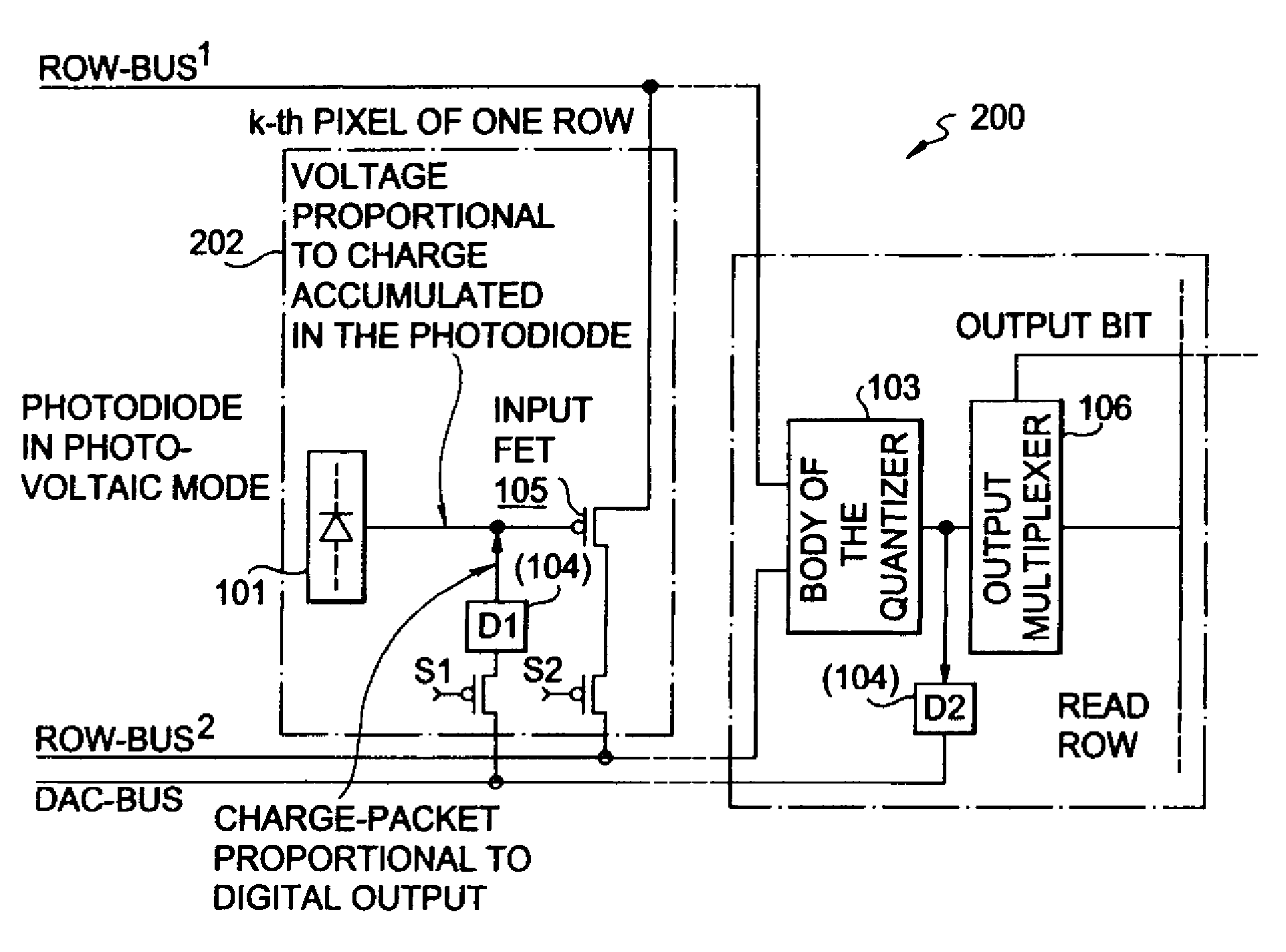
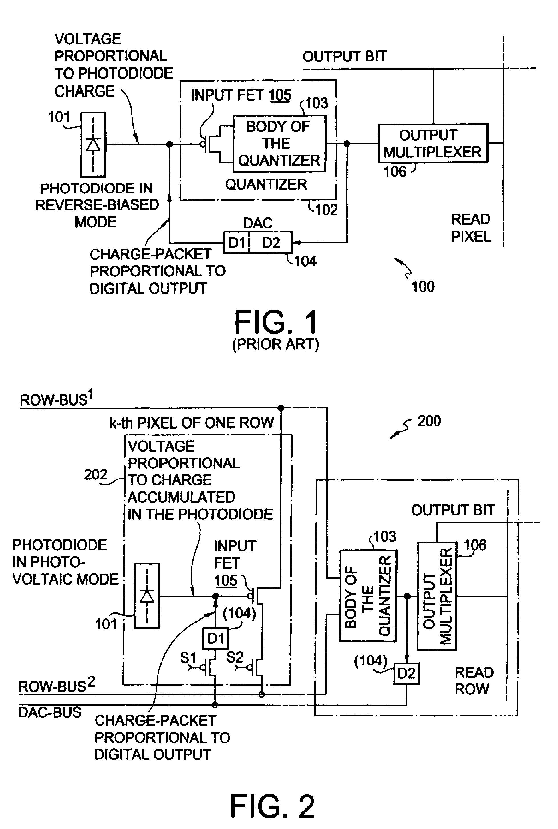
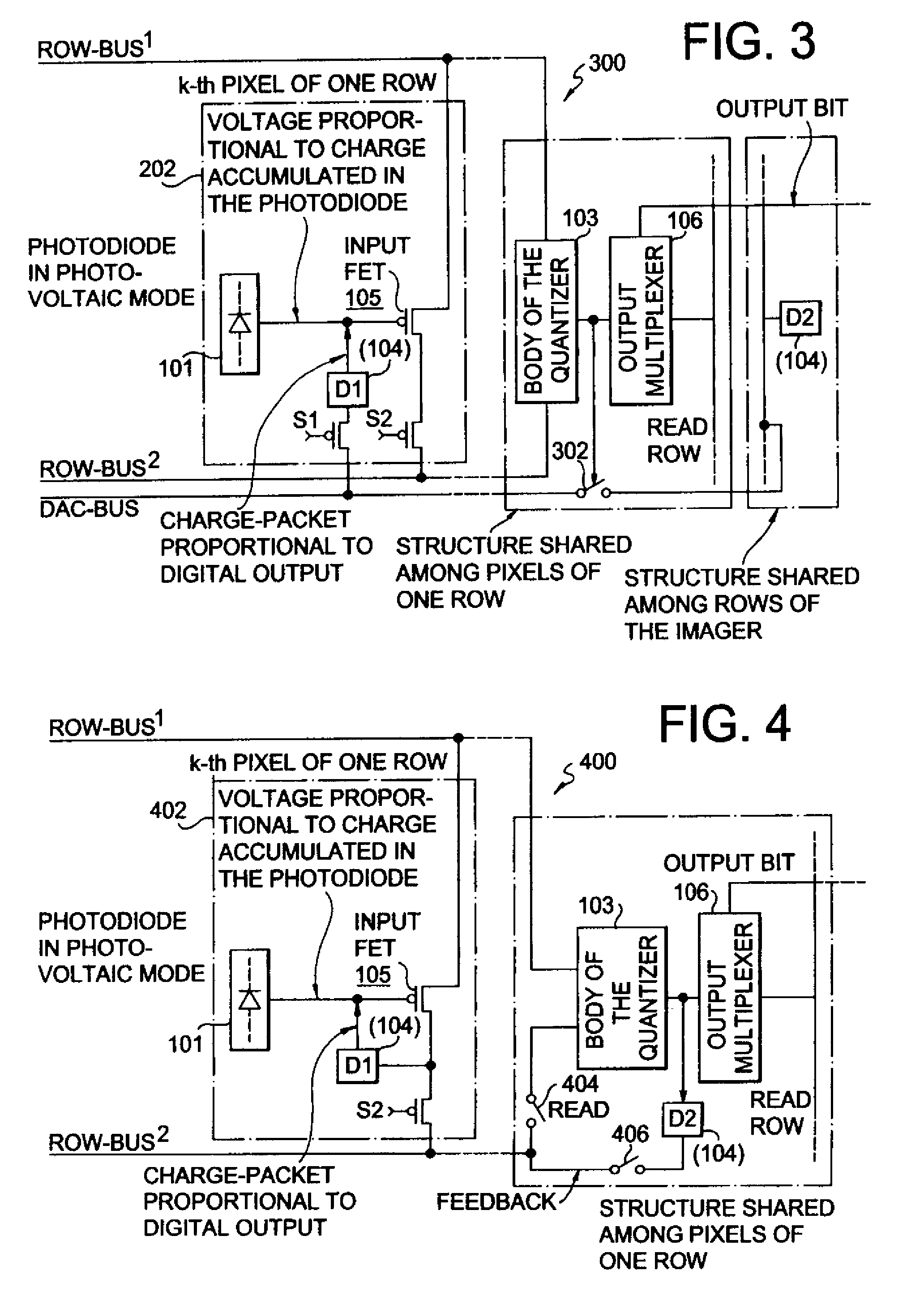
[0048]A block schematic of the known first-order pixel level ΣΔ ADC structure 100, where the integration effect of the photodiode in photo-voltaic mode is used, is shown in FIG. 1. The design shown in FIG. 1 is a fully-parallel design, meaning that each pixel is provided with separate ΣΔ ADC. The block 101 that represents the photosensitive elements contains the photodiode and possibly a biasing circuit to keep the photodiode in the photo-voltaic mode (e.g., a reset switch). While in the photovoltaic mode, the terminals of the photodiode are floating and the photo-generated charge that is built up inside the photo-diode is proportional to light intensity. The terminal voltage of the photodiode is proportional to the charge, and as such it is proportional to the light intensity. In conversion mode, when the Σ...


PUM


Abstract

In an array of imaging elements, a pixel level analog-to-digital-converter design splits the quantizer into an input transistor at the pixel location and a quantizer body for each row. The feedback digital-to-analog converter is also split into two components, one at the pixel location and one provided either for each row or for the entire array.

Description

REFERENCE TO RELATED APPLICATION[0001]The present application claims the benefit of U.S. Provisional Patent Application No. 60 / 737,418, filed Nov. 17, 2005, whose disclosure is hereby incorporated by reference in its entirety into the present disclosure.FIELD OF THE INVENTION[0002]The present invention is directed to a sigma-delta (ΣΔ) analog-to-digital converter (ADC) design and more particularly to a multiplexed-input-separated (MIS) ΣΔ ADC design adapted for use as a pixel-level ADC in a pixel readout circuit employed in a CMOS image sensors.DESCRIPTION OF RELATED ART[0003]Charge-coupled-device (CCD) imagers were first developed in the 1970's in the defense sector but quickly found acceptance among professional astronomers when they began using CCD cameras instead of photographic films and plates. There were several advantages that favored CCD cameras over photographic film:[0004]CCD cameras are up to 100 times more sensitive than film;[0005]CCD images are readily digitized, elim...

Claims


Application Information

Patent Timeline
IPC IPC(8): H03M3/00
CPCH01L27/14609H04N5/335H03M3/474H03M3/33H03M3/456H04N25/00
Inventor IGNJATOVIC, ZELJKOBOCKO, MARK F.
Owner UNIVERSITY OF ROCHESTER
Why Eureka
Try Eureka