Temperature compensated dynamic optical tag modulator system and method

a dynamic optical tag and modulator technology, applied in the field of temperature compensation dynamic optical tag modulator system and method, can solve the problems of difficult manufacturing of quantum well optical modulators having high breakdown voltage, difficult to manufacture electro-absorption optical modulators that are able, and temperature dependent modulation characteristics, etc., to reduce the dc bias required to tune the optical modulator

Active Publication Date: 2009-10-13
CUBIC CORP
View PDF28 Cites 17 Cited by
  • Summary
  • Abstract
  • Description
  • Claims
  • Application Information

AI Technical Summary

Benefits of technology

[0010]A transmissive quantum well optical modulator mounted on the front surface of a retro-reflector (corner cube) in the remote receiver end (Tag) of the communication link is biased to optimize the modulation of one of the two laser wavelengths. At higher temperatures, the optical modulator can be biased to operate at the wavelength of one of the two lasers. At a lower temperature, the optical modulator can be biased to operate at the second of the two wavelengths. The DC bias required to tune the optical modulator is reduced by operating at two separate wavelengths depending on the temperature of the modulator.

Problems solved by technology

A drawback to such modulators is that their modulation characteristics are quite temperature dependent.
It is extremely difficult to manufacture a quantum well optical modulator having a high breakdown voltage.
In particular, it is difficult to manufacture an electro-absorption optical modulator that is able to withstand an 90 volt reverse voltage bias at a high manufacturing yield.
Increasing the yield of high breakdown voltage optical modulators would likely entail complex Metal-Organic Chemical Vapor Deposition (MOCVD) growth processes and epitaxial wafer design controls.
The technology and development time and costs required to produce a high breakdown voltage optical modulator makes it unsuitable for application in optical communication systems that require immediate low cost solutions.

Method used


Image

  • Temperature compensated dynamic optical tag modulator system and method
  • Temperature compensated dynamic optical tag modulator system and method
  • Temperature compensated dynamic optical tag modulator system and method

Examples


Embodiment Construction

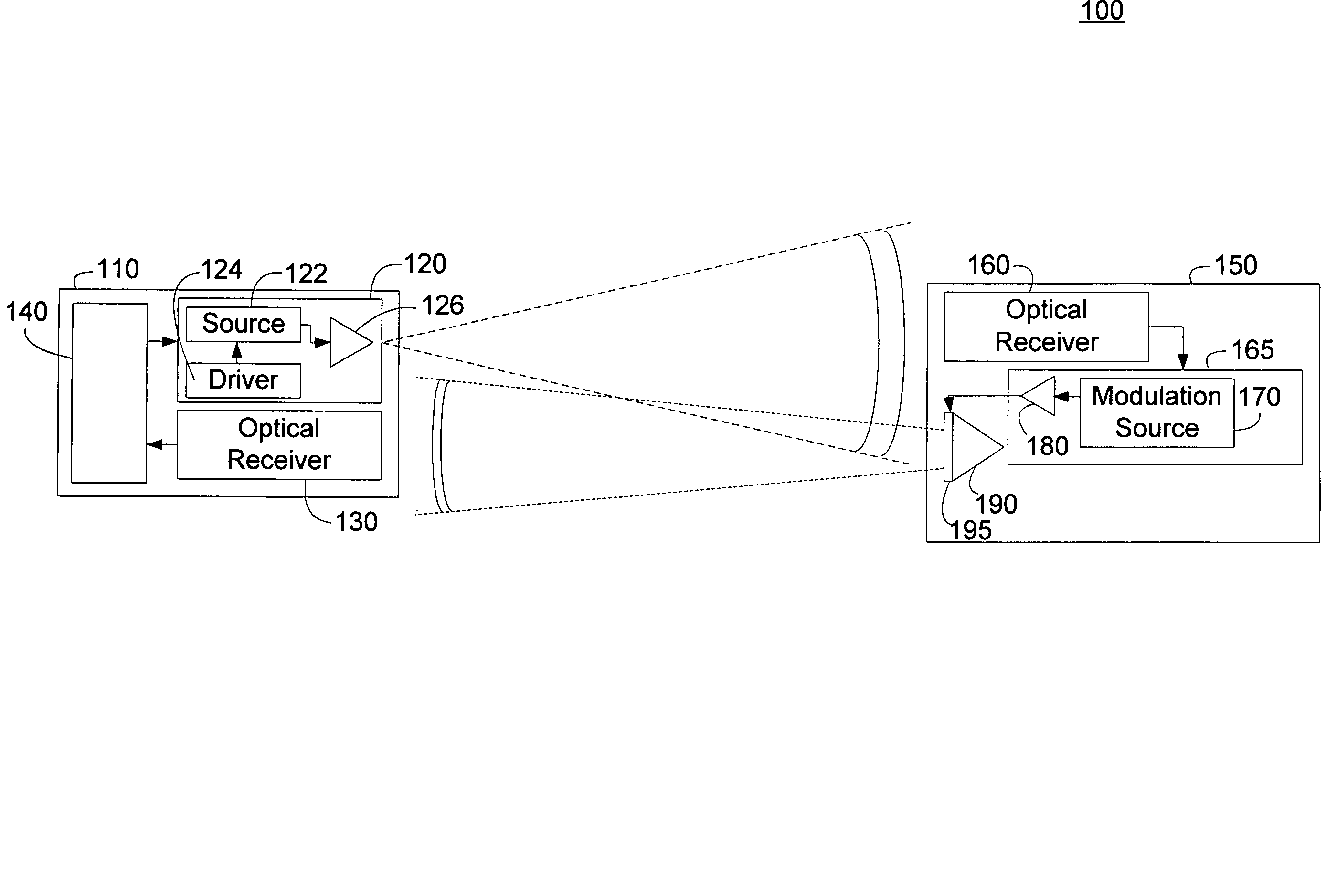
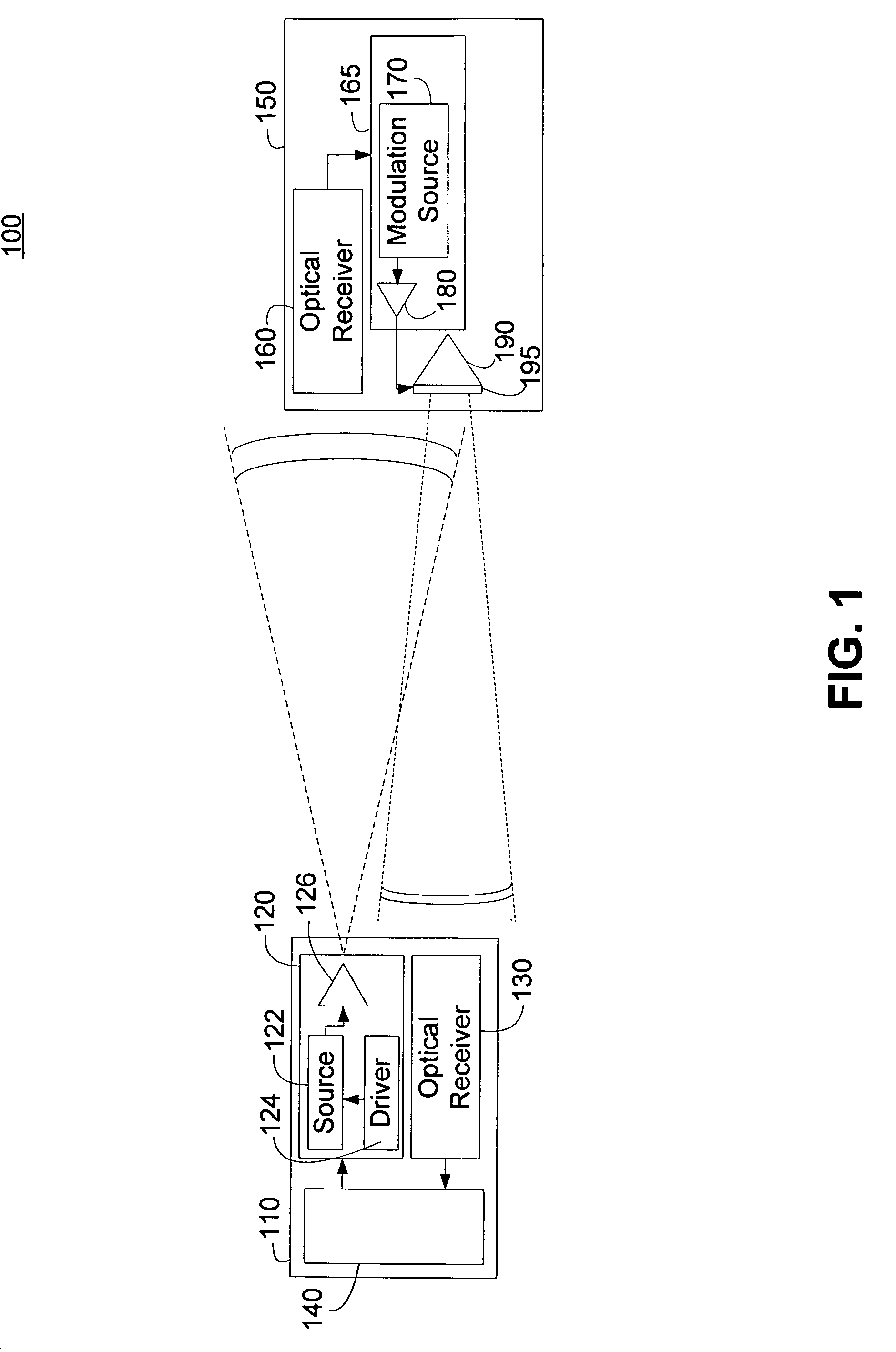
[0024]An optical transmitter and method of generating a pulsed optical output for a Dynamic Optical Tag (DOT) system that is configured to operate over an extended temperature range is disclosed. The pulsed optical output can be received by a remote Tag, where the received optical signal is retro-modulated by an optical modulator and reflected back to the optical transmitter. The DOTs system can be implemented using an optical modulator having a reduced reverse breakdown voltage requirement. The lower reverse breakdown voltage requirement allows for a greater yield of optical modulators and a reduced manufacturing cost. A quantum well modulator having the reduced reverse breakdown voltage requirements can be manufactured with a yield exceeding 70% while quantum well modulators requiring reverse breakdown voltages of 90 volts or greater typically have a manufacturing yield less than 10%.

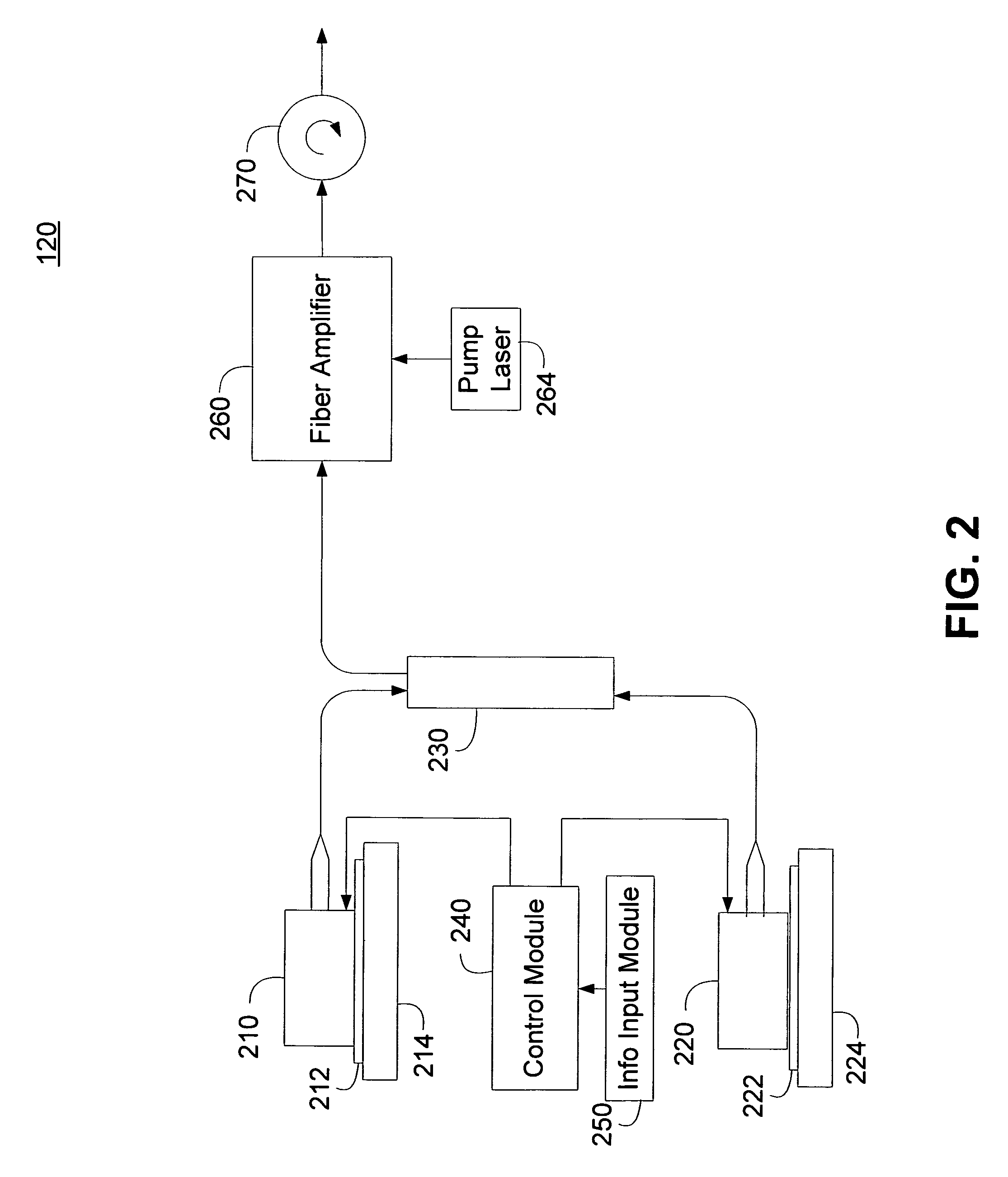
[0025]The optical source can use two Distributed Feedback (DFB) lasers operating at distinct wavel...


PUM


Abstract

A dynamic optical tag system and method that allows for operation over a wide temperature range. A variable wavelength optical source, such as a dual wavelength fiber laser, is generated by combining the outputs from two distributed feedback lasers having separate operating wavelengths using a wavelength division multiplexer (WDM). A quantum well optical modulator mounted on the front surface of a retro-reflector in the remote receiver end of the communication link is biased to modulate one of the two laser wavelengths. At higher temperatures, the optical modulator can be biased to operate at the wavelength of one of the two lasers. At a lower temperature, the optical modulator can be biased to operate at the second of the two wavelengths. The DC bias required to tune the optical modulator is reduced by operating at two separate wavelengths depending on temperature.

Description

STATEMENT AS TO RIGHTS TO INVENTIONS MADE UNDER FEDERALLY SPONSORED RESEARCH OR DEVELOPMENT[0001]This invention was made with government support under Contract Number H92222-04-C-0004 awarded by the United States Special Operations Command. The government has certain rights in the invention.BACKGROUND OF THE INVENTION[0002]An optical communication system, such as a free space optical communication system, can use modulated optical signals to convey information. The optical signal can be generated by an optical source having a relatively narrow spectral bandwidth, such as a laser.[0003]A laser optical source can be optically modulated using any one of a variety of methods. For example, the laser output can be optically modulated internal to the laser by modulating a current to the laser. The current can affect the light intensity of the laser output according to a characteristic light to current curve. An alternative to internally modulating the bias current of the laser is to utiliz...

Claims


Application Information

Patent Timeline
Patent Type & Authority Patents(United States)
IPC IPC(8): H04B10/00
CPCH04B10/1123
Inventor VARSHNEYA, DEEPAKJEFFERS, LARRY
Owner CUBIC CORP
Why Eureka
Try Eureka