System for reading and writing on flash memory device having plural microprocessors

a flash memory device and microprocessor technology, applied in the field of data storage devices, can solve the problems of inflexibility of most such systems to be scaled up, the performance speed of read and write operations is less than the desired speed, and the system is difficult to scale up to a larger, robust system, etc., to achieve less ram and bus contention issues, less expensive implementation, and better performance

Active Publication Date: 2011-04-19
INTELLECTUAL VENTURES II
View PDF10 Cites 24 Cited by
  • Summary
  • Abstract
  • Description
  • Claims
  • Application Information

AI Technical Summary

Benefits of technology

[0021]The inventor conceptualized and subsequently provided a Flash data storage device constructed using a distributive architecture that was less expensive to implement and had fewer RAM and bus contention issues than single processor devices. The result was a better performance relative to data management speeds including reads and writes.

Problems solved by technology

One of several problems stated above is that it in computing where data storage is involved it is difficult to scale up to larger more robust system using a device having a single processor for managing all of the Flash data management operations over a shared bus system.
However, existing systems use a single complex processor over a shared bus to access the Flash media for read and write access.
The result is a less than desired performance speed for read and write operations due to RAM and bus contentions by the various data management process components.
Most such systems are not flexible enough to be scaled up for enterprise applications that might use Flash media as the persistent storage medium because of bus and RAM contentions.
Moreover, larger more complex processors are expensive and although capable of the data management tasks required of enterprise systems, suffer degradation of performance speed at levels of higher utilization.

Method used


Image

  • System for reading and writing on flash memory device having plural microprocessors
  • System for reading and writing on flash memory device having plural microprocessors
  • System for reading and writing on flash memory device having plural microprocessors

Examples


Embodiment Construction

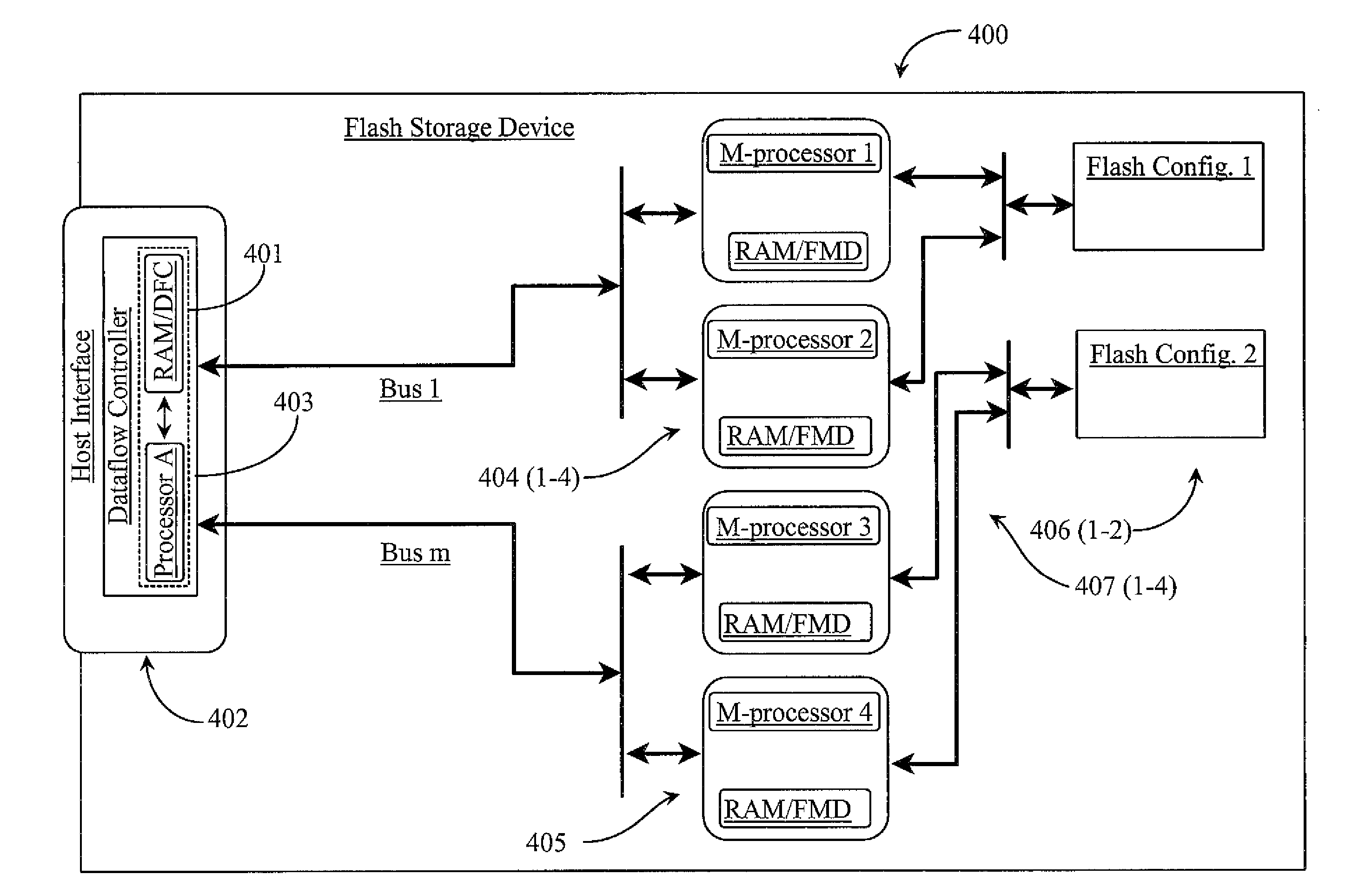
[0032]The inventor provides a multiple processor flash-based storage device and a system for managing data relative to use of the device for data storage. The invention is enabled in detail according to the following embodiments.

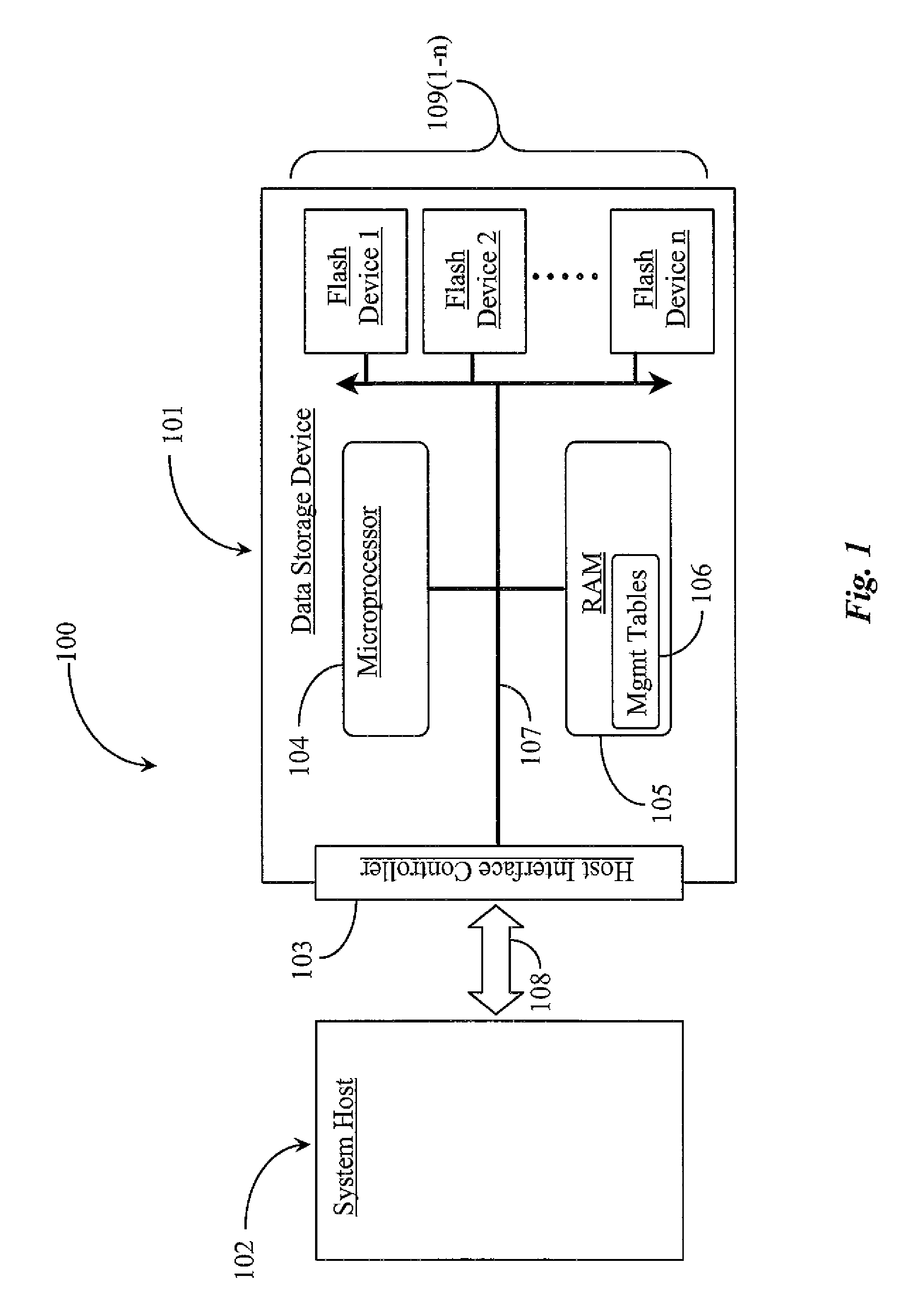
[0033]FIG. 1 is a block diagram illustrating a single-processor Flash storage device as known to the inventor. In this system known to the inventor and briefly described above in the background section of this specification, a single processor is used to perform all of the functions relative to reading and writing data to one or more Flash-based storage devices.

[0034]In the system of FIG. 1 data storage system 100 includes a data storage device 101 and a host computing device 102. Host computing device 102 may be a personal computer (PC) or a hand-held device such as a personal digital assistant (PDA), a Laptop computer, or some other computing device that can be coupled to data storage device 101 for the purpose of reading data from and writing data to the ...


PUM


Abstract

A system for writing and reading data includes a controller accessible to at least one or more computing systems, a plurality of microprocessor units accessible to the controller, and a plurality of memory device configurations each having one dedicated bus connection to individual ones or multiples of the microprocessor units. The controller receives write and read requests from the one or more computing systems and selects which of the plurality of microprocessor units will write or read data associated with the requests.

Description

CROSS-REFERENCE TO RELATED APPLICATIONS[0001]The present invention is a continuation-in-part (CIP) to a U.S. patent application Ser. No. 11 / 439,619, filed on May 23, 2006, now U.S. Pat. No. 7,464,240, entitled “Hybrid Solid State Disk Drive with Controller”, to a U.S. patent application Ser. No. 11 / 439,620, filed on May 23, 2006, now U.S. Pat. No. 7,461,229, entitled “Software Program for Managing and Protecting Data Written to a Hybrid Solid State Disk Drive”, and to a U.S. patent application Ser. No. 11 / 439,615, filed on May 23, 2006, now U.S. Pat. No. 7,424,587, entitled “Methods for Managing Data Writes and Reads to a Hybrid Solid State Disk Drive”, disclosures of which are incorporated in their entireties at least by reference.BACKGROUND OF THE INVENTION[0002]1. Field of the Invention[0003]The present invention is in the field of data storage devices including disk drives and mass storage systems and pertains particularly to processor-based data storage devices and systems for ...

Claims


Application Information

Patent Timeline
Patent Type & Authority Patents(United States)
IPC IPC(8): G06F12/00
CPCG06F13/1694
Inventor CAULKINS, JASON
Owner INTELLECTUAL VENTURES II
Why Eureka
Try Eureka