

Method and system for lithography using phase-change material
a phase-change material and lithography technology, applied in the field of manufacturing optical memory devices, can solve the problems of difficult to provide a source/drain current of more than 1 ma for a minimum size device, large optical system, and high cost compared to the media
- Summary
- Abstract
- Description
- Claims
- Application Information
AI Technical Summary
Benefits of technology
Problems solved by technology
Method used
Image

Examples
Embodiment Construction
[0001] 1. Field of the Invention
[0002] The invention relates to manufacturing integrated circuits in general, and to manufacturing optical memory devices in particular.
[0003] 2. Background of the Invention
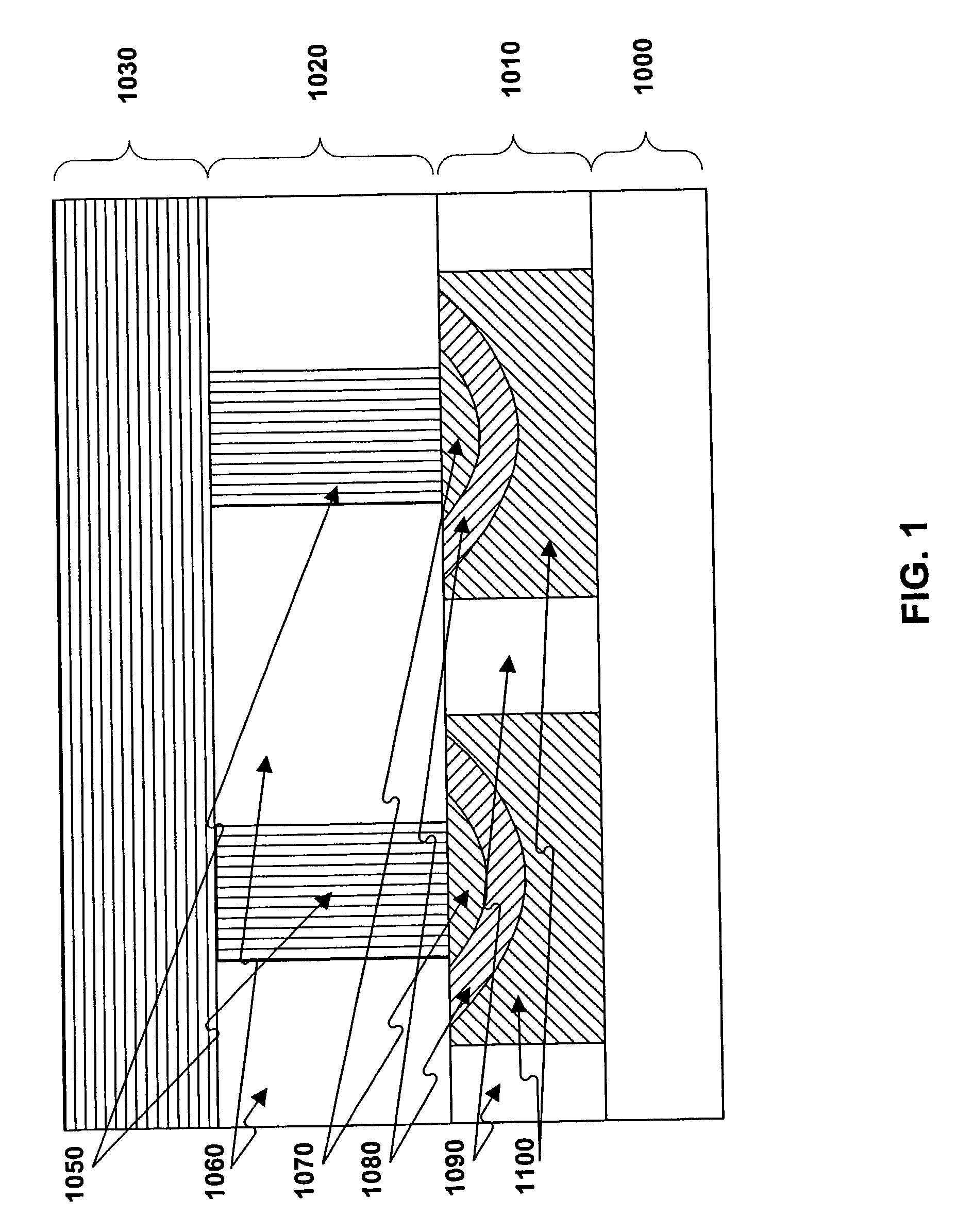
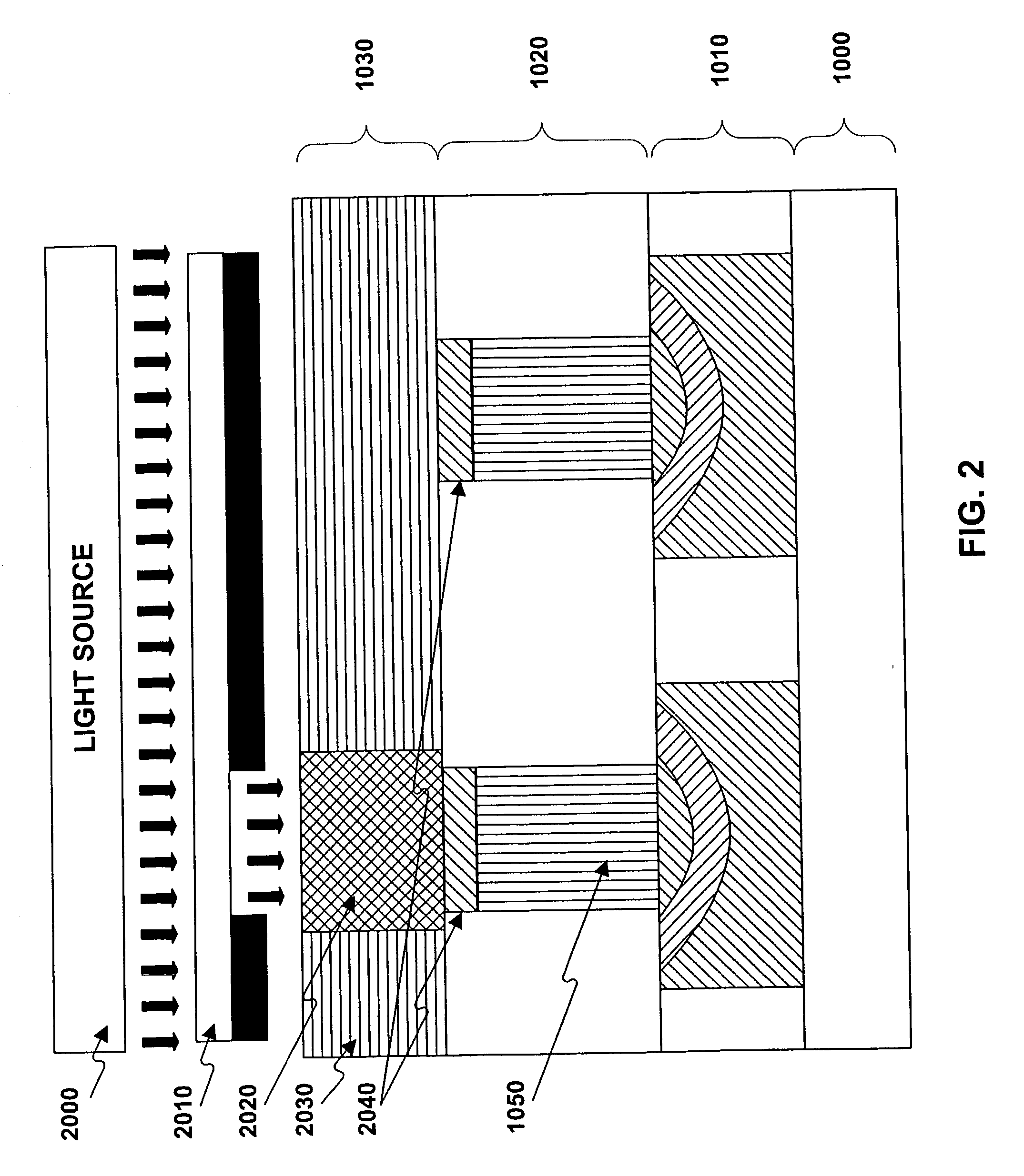
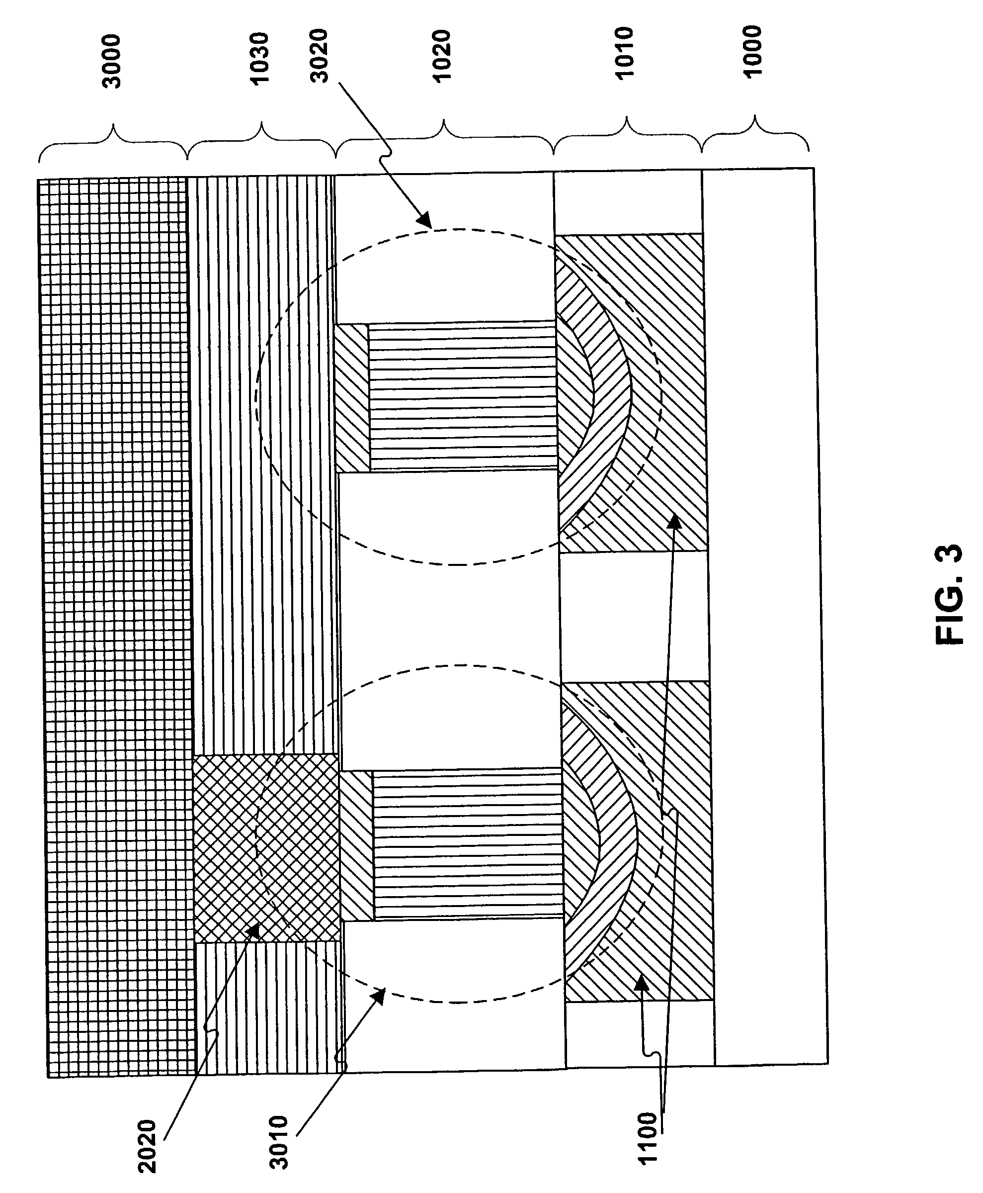
[0004] Phase change materials may be switched from one detectable state to another detectable state by the application of energy. The states of phase change materials may differ in their morphology, relative degree of order, or relative degree of disorder, creating a detectable difference in electrical conductivity, electrical resistance, optical transmissivity, optical absorption, optical reflectivity, or any combination thereof.
[0005] Conventional systems for using phase-change material, such as chalcogenide, to implement optical data storage media may be classified into two categories. The first category includes media that are optically read and written, such as CD-Rewritable (CD-RW) memory, Powerful Optical Disk System (PD) memory, and Digital Versatile Disk RAM (DVD-RAM). The...
PUM
| Property | Measurement | Unit |
|---|---|---|
| current | aaaaa | aaaaa |
| source/drain current | aaaaa | aaaaa |
| thickness | aaaaa | aaaaa |
Abstract
Description
Claims
Application Information