
Method and system for waveguide mode filters
a waveguide mode and filter technology, applied in the field of signal processing, can solve the problems of cable bulk penalties, large power requirements, and complex structure, and achieve the effects of small improvement in reach, limited scalability, and limited application rang
- Summary
- Abstract
- Description
- Claims
- Application Information
AI Technical Summary
Benefits of technology
Problems solved by technology
Method used
Image

Examples
Embodiment Construction
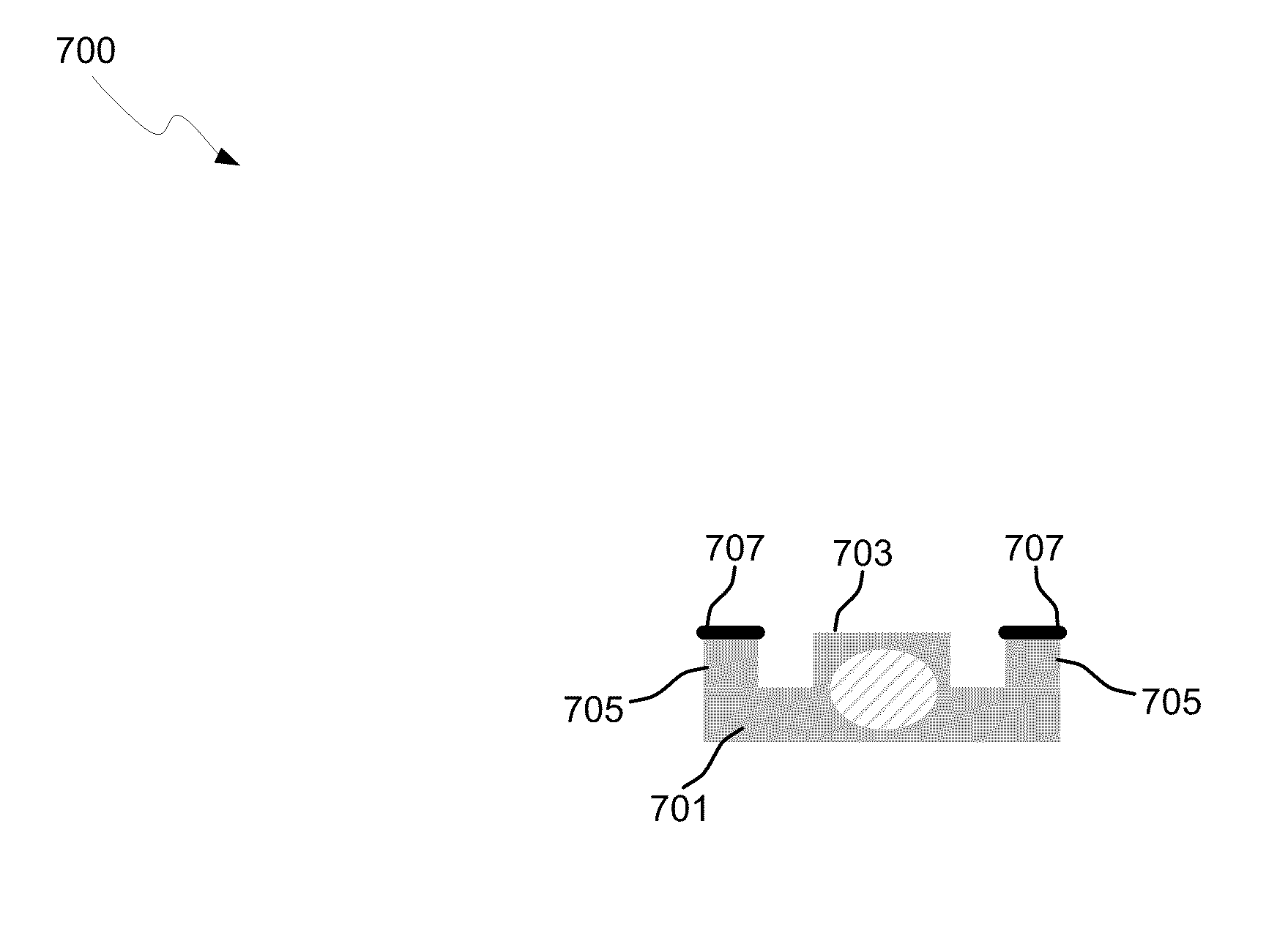
[0019]Certain aspects of the invention may be found in a method and system for waveguide mode filters. Exemplary aspects of the invention may comprise processing optical signals of a fundamental mode and higher order modes by filtering the higher-order modes in rib waveguides in a photonic chip. The higher-order modes may be filtered utilizing doped regions and / or patterns in one or more slab sections in the rib waveguides. The patterns may be periodic or aperiodic along the rib waveguides. The higher-order modes may be filtered utilizing varying widths of slab sections, or doped, patterned, and / or salicided ridges on the slab sections in the rib waveguides. The higher-order modes may be attenuated by scattering and / or absorbing the modes. The chip may comprise a CMOS photonic chip.
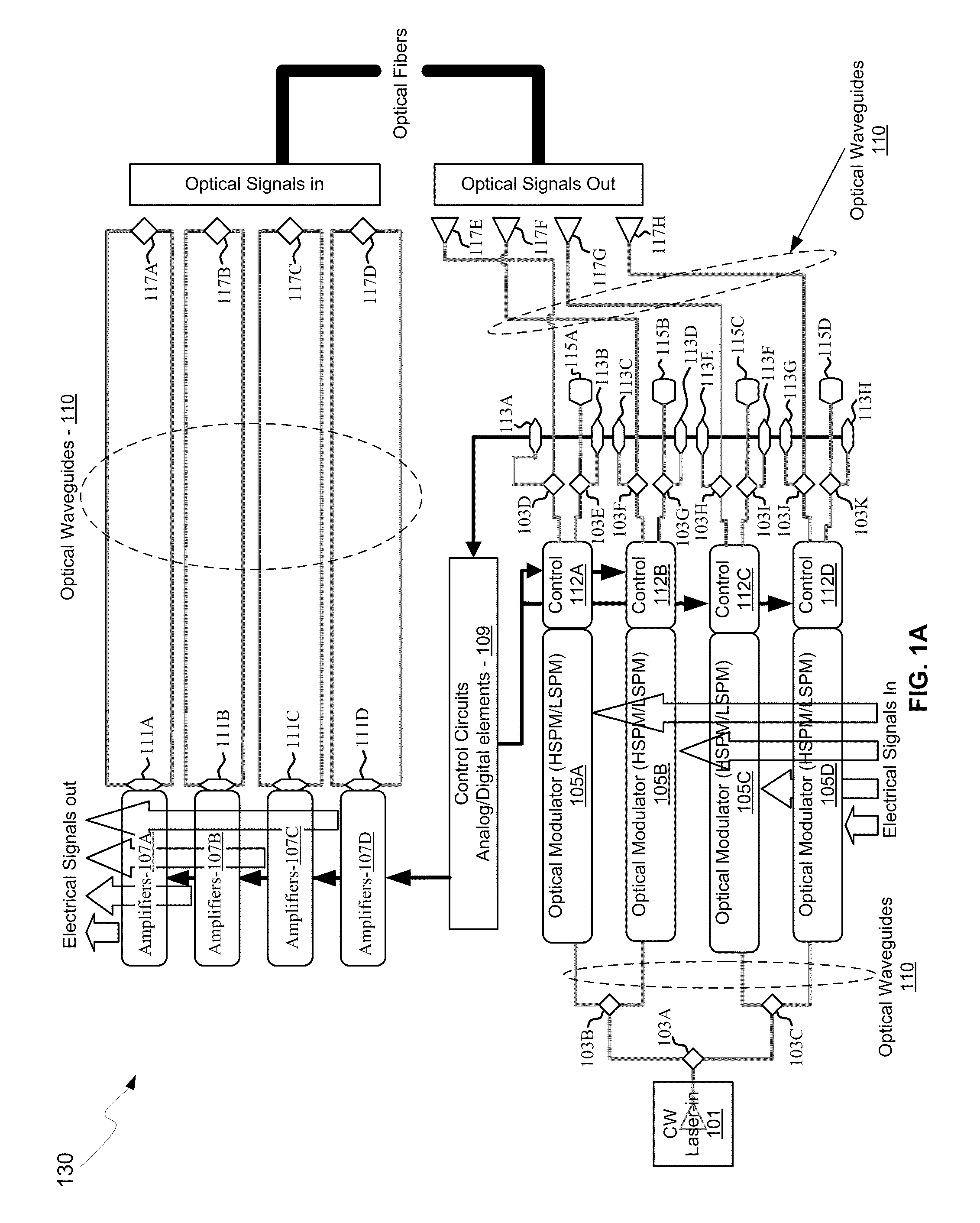
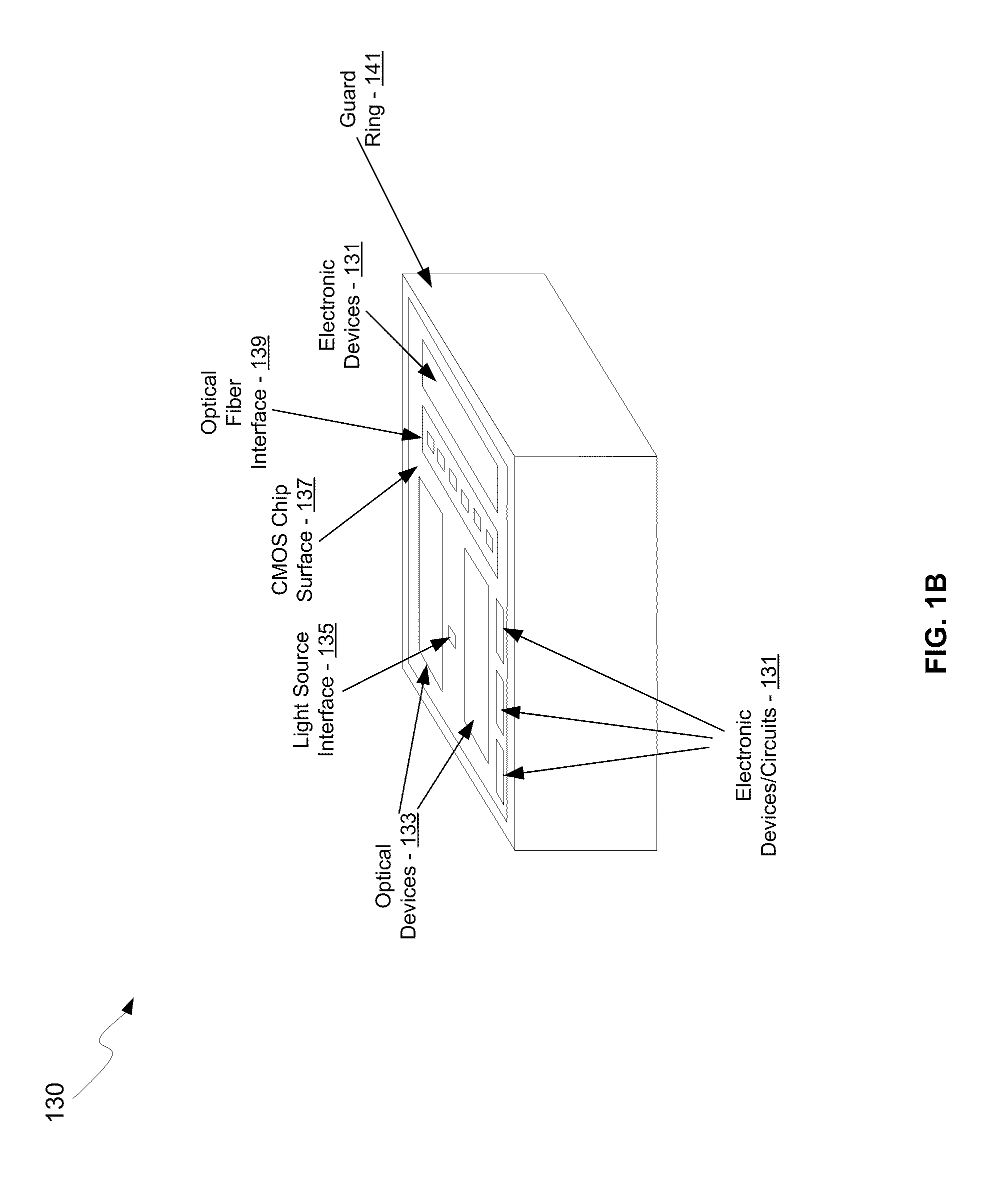
[0020]FIG. 1A is a block diagram of a photonically enabled CMOS chip comprising waveguide mode filters, in accordance with an embodiment of the invention. Referring to FIG. 1A, there is shown optoelectron...
PUM
 Abstract
Description
Claims
Application Information