
Low latency multi-detector noise cancellation
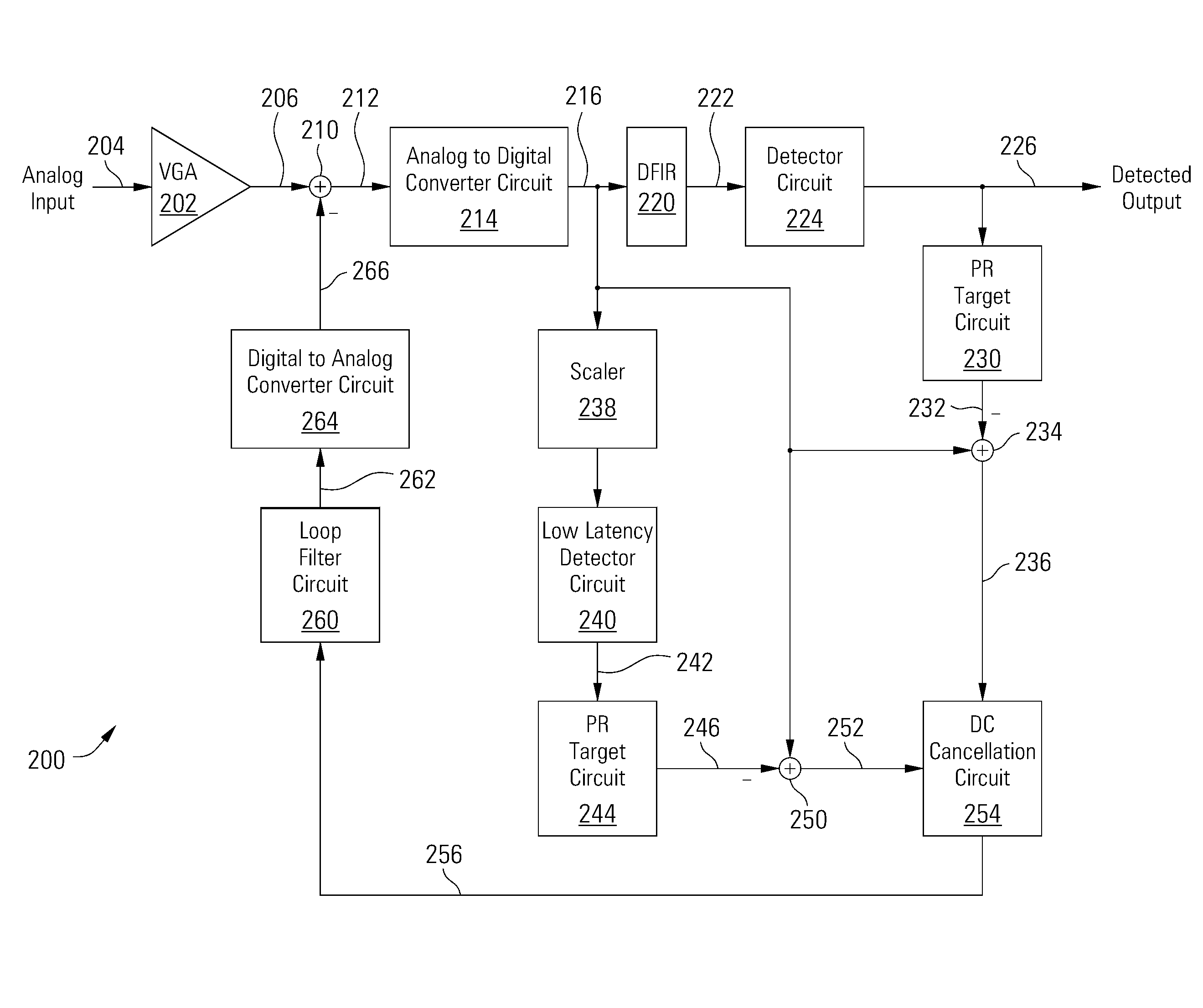
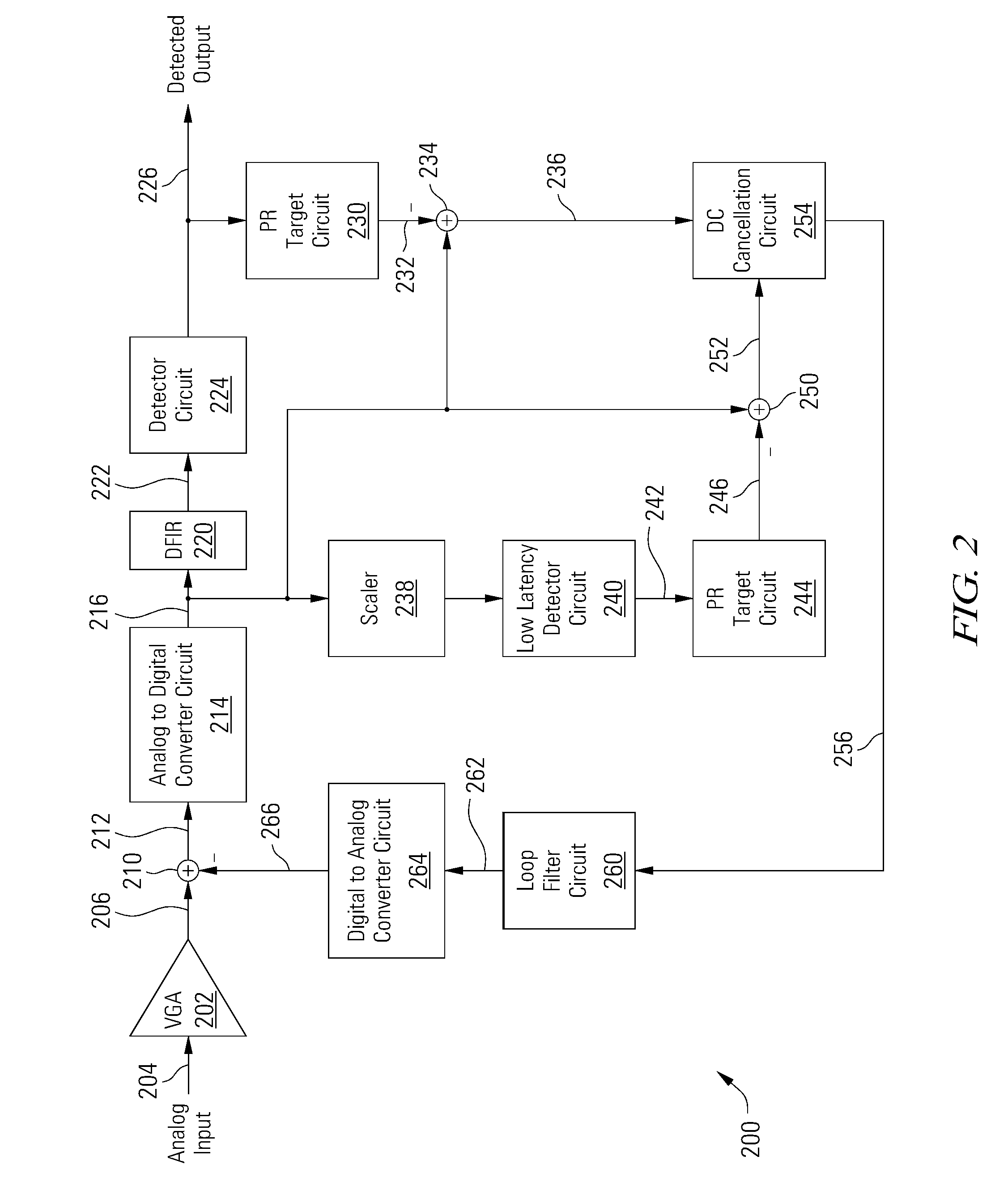
a multi-detector, low-latency technology, applied in the field of data processing, can solve problems such as large loop noise, and achieve the effect of reducing interferen
- Summary
- Abstract
- Description
- Claims
- Application Information
AI Technical Summary
Benefits of technology
Problems solved by technology
Method used
Image

Examples
Embodiment Construction
[0022]Various embodiments of the present invention are related to systems and methods for data processing, and more particularly to systems and methods for low latency loop processing.
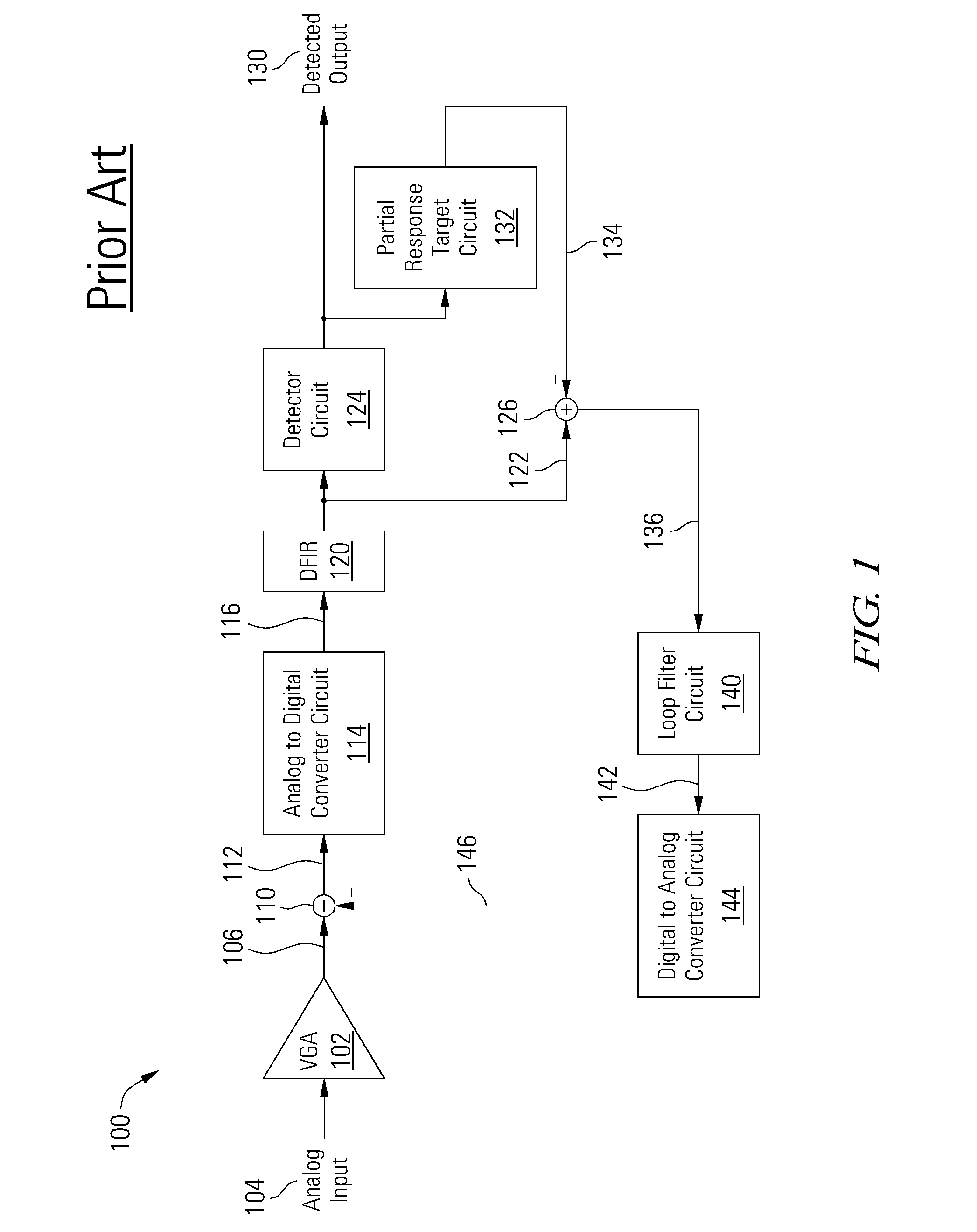
[0023]Turning to FIG. 1, an existing loop circuit 100 is shown that includes low frequency noise correction feedback. Loop circuit 100 includes a variable gain amplifier (VGA) 102 that receives an analog input 104. Variable gain amplifier 102 amplifies analog input 104 to yield an amplified output 106 that is provided to a summation circuit 110. Summation circuit 110 subtracts a feedback signal 146 from amplified output 106 to yield a sum 112.
[0024]Sum 112 is provided to an analog to digital converter circuit (ADC) 114 that converts the received signal into a series of digital samples 116 that are provided to a digital finite impulse response (DFIR) filter 120. Digital finite impulse response filter 120 acts as an equalizer and filters the received input to provide a corresponding filtered output 122 t...
PUM
| Property | Measurement | Unit |
|---|---|---|
| length | aaaaa | aaaaa |
| frequency | aaaaa | aaaaa |
| frequency noise | aaaaa | aaaaa |
Abstract
Description
Claims
Application Information