Optical element unit and method of supporting an optical element

a technology of optical elements and optical elements, applied in the field of optical element units, can solve the problems of affecting the stability the inability to adjust the position of the lens relative to the holder at reasonable small effort, and the introduction of stresses into the optical element, etc., to achieve good and long-term stable and reliable imaging properties of the optical system

Active Publication Date: 2015-09-15
CARL ZEISS SMT GMBH
View PDF30 Cites 4 Cited by
  • Summary
  • Abstract
  • Description
  • Claims
  • Application Information

AI Technical Summary

Benefits of technology

[0014]It is thus an object of the invention to, at least to some extent, overcome the above disadvantages and to provide good and long-term stable and reliable imaging properties of an optical system, in particular of an optical system used in an exposure process.
[0015]It is a further object of the invention to easily and reliably reduce the introduction of stresses into the optically used area of an optical element used in an exposure process.
[0016]These objects are achieved according to the invention which is based on the teaching that good and long term reliable imaging properties may be achieved if, on the one hand, connector elements are provided having a first connector part contacting the optical element and a second connector part contacting the optical element holder and preventing rotation between the first connector part and the second connector part in a plane substantially parallel to the plane of main extension of the optical element. Preventing such a rotation also prevents the introduction of deformation and pre-stresses, e.g. resulting from fastening torques etc., into the parts connecting the first connector part and the second connector part and, thus, into the optical element.
[0017]On the other hand, the invention is based on the teaching that good and long term reliable imaging properties may be achieved if, on the other hand, in an optical element unit, the same plurality of connector elements is provided for a number of optical elements defining an optical element unit axis and the connector elements of one of this a plurality of optical elements are rotated about said optical element unit axis with respect to the connector elements of another one of this a plurality of optical elements in order to compensate for deformation induced imaging errors. The angle of relative rotation between the connector elements of different optical elements depends on the number of connector elements and the number of optical elements participating in the compensation. It will be appreciated that, by this rotation, the imaging errors due to the mass induced deformation of the respective optical element may at least partially compensate each other such that the overall imaging error of the optical system is at least reduced.
[0018]Thus, according to a first aspect of the invention there is provided an optical element unit comprising an optical element, a connector element, and an optical element holder. The optical element has a plane of main extension as well as an outer circumference and defines a radial direction. The connector element connects the optical element and the optical element holder, the connector element having a first connector part connected to the optical element at the outer circumference and a second connector part connected to the optical element holder. The first connector part and the second connector part are connected via at least one coupling part, the coupling part being compliant in the radial direction and substantially preventing rotation between the first connector part and the second connector part in a plane substantially parallel to the plane of main extension.
[0025]According to a seventh aspect of the invention there is provided a method of supporting an optical element comprising, in a first step, providing the optical element and an optical element holder, the optical element having a plane of main extension as well as an outer circumference and defining a radial direction. In a second step, a connector element is provided and the optical element and the optical element holder are connected via the connector element, the connector element having a first connector part connected to the optical element at the outer circumference and a second connector part connected to the optical element holder. The first connector part and the second connector part are connected so as to provide compliance in the radial direction and to substantially prevent rotation between the first connector part and the second connector part in a plane substantially parallel to the plane of main extension.

Problems solved by technology

One of the problems arising in the context of imaging accuracy is the introduction of stresses into the optical elements via the elements holding the respective optical element.
A connection that is rigid in the direction of this thermally induced shift leads to an introduction of considerable stresses into the optical element.
In the optical exposure systems mentioned above, this problem mainly arises in the radial direction of the optical element, i.e. in or parallel to the plane of main extension of the optical element.
However, this solution has the disadvantage that, once the adhesive bonding of the lens and the holder is achieved, virtually no further correction or adjustment of the position of the lens relative to the holder is possible anymore at reasonably small effort.
However, this solution has the disadvantage that considerable effort is necessary when mounting the connector elements to the holder ring in order to avoid introduction of pre-stresses and deformations into the leaf spring elements, e.g. due to fastening torques, which may otherwise lead to the introduction of additional stresses into the optical element.
Such stresses introduced into the optical element may cause local anisotropies within the material of the optical element leading to so called stress induced birefringence effects.
Among others, such birefringence alters polarization of the light which is of particular disadvantage when occurring in an illumination system.
This is due to the fact that, usually, no active cooling circuitry is provided for the illumination system.
In general, birefringence effects and deformations of the optical elements deteriorate the optical performance of the optical system.
While such an intermediate support ring provides enough space for a reduction of the stresses introduced into it via the external support structure, it has the disadvantage that it is rather costly due to the necessary adaptation of its coefficient of thermal expansion.
Furthermore, it introduced a further interface location and, thus, further positioning errors.

Method used


Image

  • Optical element unit and method of supporting an optical element
  • Optical element unit and method of supporting an optical element
  • Optical element unit and method of supporting an optical element

Examples


first embodiment

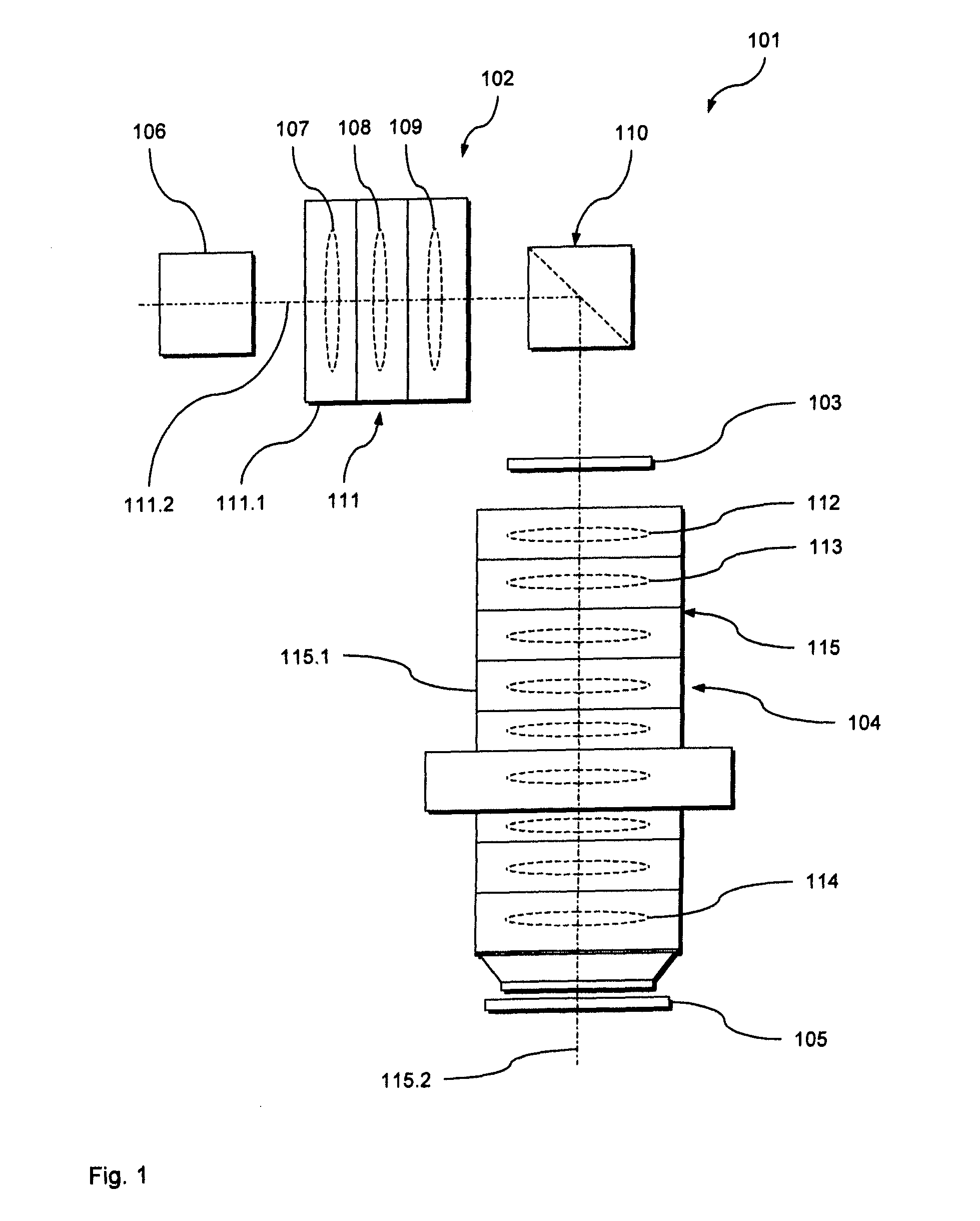
[0046]In the following, a first preferred embodiment of an optical exposure apparatus 101 according to the invention comprising an illumination system 102, a mask 103, an optical projection system 104 and a substrate 105 will be described with reference to FIGS. 1 to 6.

[0047]The optical exposure apparatus 101 is adapted to transfer an image of a pattern formed on the mask 103 onto the substrate 105. To this end, the illumination system 102 illuminates the mask 103 with exposure light. The optical projection system 104 projects the image of the pattern formed on the mask 103 onto the substrate 105, e.g. a wafer or the like.

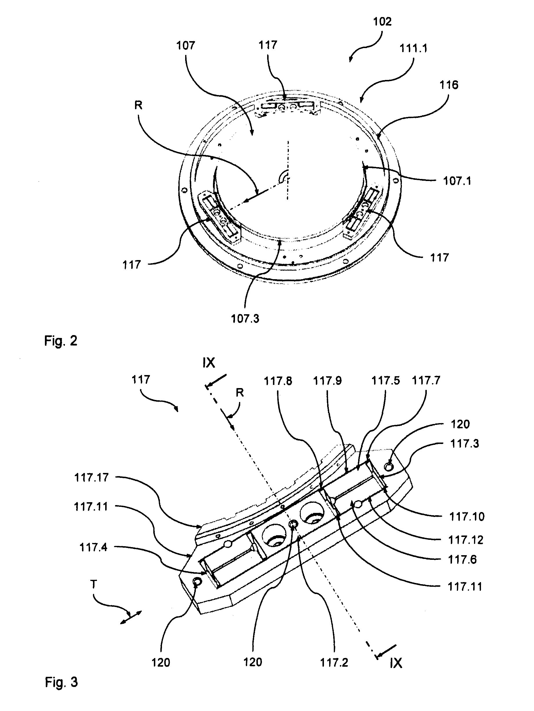
[0048]To this end, the illumination system 102 comprises a light source 106 and a plurality of optical elements 107 to 110, such as lenses, mirrors, gratings or the like. The optical elements 107 to 109 are held within a first housing 111.1 of a first optical element unit 111 according to the invention. The optical elements 107 to 110 cooperate to define the beam o...

second embodiment

[0080]In the following, a second preferred embodiment of an optical element unit according to the invention in the form of the second optical element unit 115 will be described with reference to FIGS. 1 and 8.

[0081]FIG. 8 shows a schematic partial view of the second optical element unit 115 from above along the second optical element unit axis 115.2. More specifically, FIG. 8 shows a schematic view of a first optical element in the form of lens 112 with its first connector elements 129 mounted to a first holder 130 and a second optical element in the form of lens 113 with its second connector elements 131 mounted to a second holder 132.

[0082]The first connector elements 129 and the second connector elements 131 correspond to the connector elements 117 such that, with respect to their design and functionality, it is here only referred to the explanations given above with respect to the connector elements 117. Furthermore, the first holder 130 and the second holder 132 correspond to t...

third embodiment

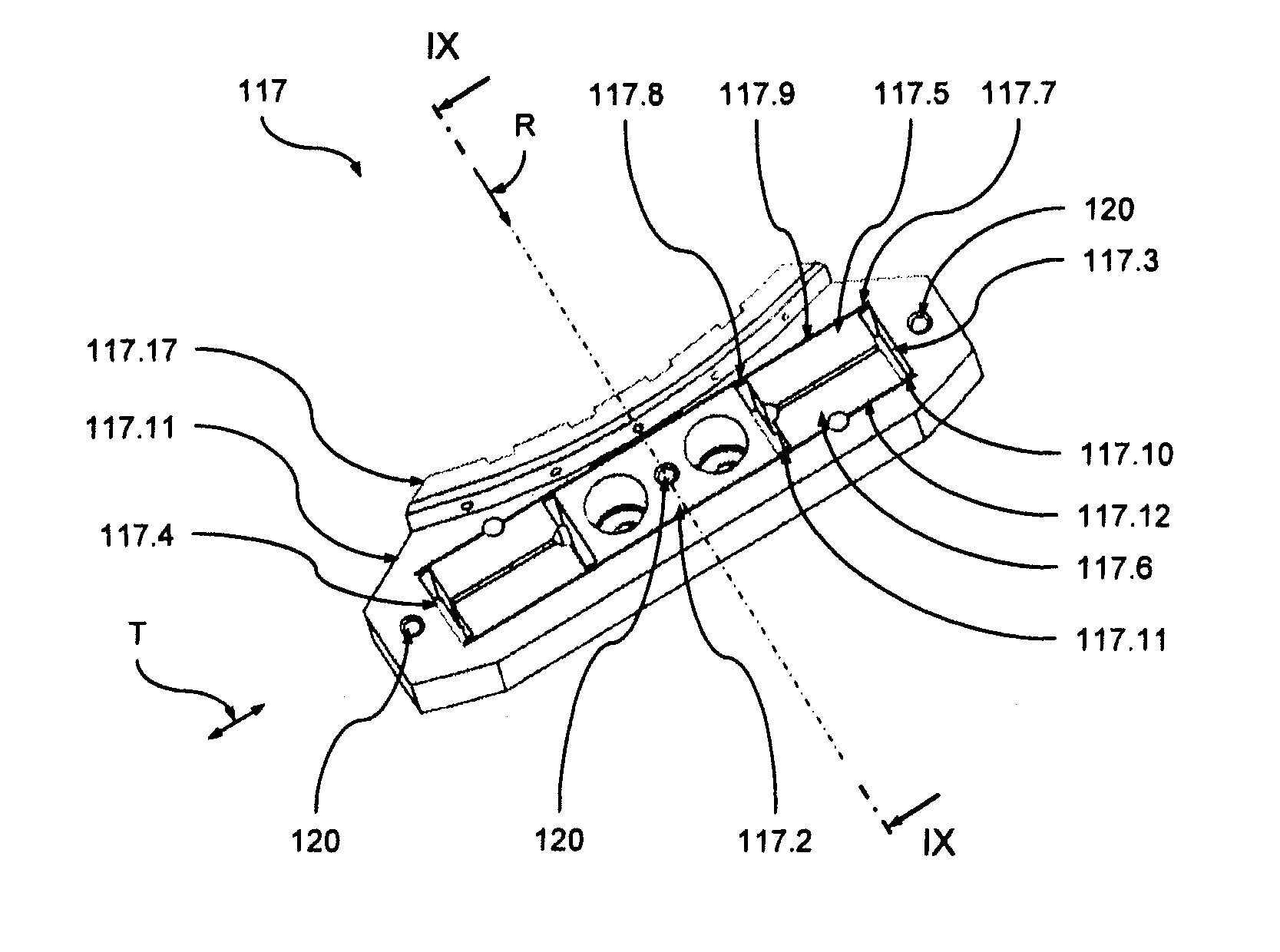
[0089]In the following, a third preferred embodiment of an optical element unit according to the invention in the form of an optical element unit 211 will be described with reference to FIGS. 1 and 9. The optical element unit 211 may replace the optical element unit 111 in the optical exposure apparatus 101 of FIG. 1. The optical element unit 211, in its basic design and functionality, largely corresponds to the optical element unit 111 such that it will here be mainly referred to the differences. In particular, like parts have been given the same reference numerals raised by the amount 100.

[0090]FIG. 9 shows a schematic partial sectional view (corresponding to a section along line IX-IX of FIG. 3) of the connector element 217 of the optical element unit 211. The only difference of the connector element 217 with respect to the connector element 117 of the optical element unit 111 lies within the design of the contact part 217.17 of the first connector part 217.1.

[0091]The first conn...


PUM

PropertyMeasurementUnit
temperatureaaaaaaaaaa
circumferenceaaaaaaaaaa
bending resistanceaaaaaaaaaa

Abstract

There is provided an optical element unit comprising an optical element, a connector element, and an optical element holder. The optical element has a plane of main extension as well as an outer circumference and defines a radial direction. The connector element connects the optical element and the optical element holder, the connector element having a first connector part connected to the optical element at the outer circumference and a second connector part connected to the optical element holder. The first connector part and the second connector part are connected via at least one coupling part, the coupling part being compliant in the radial direction and substantially preventing rotation between the first connector part and the second connector part in a plane substantially parallel to the plane of main extension.

Description

BACKGROUND OF THE INVENTION[0001]The invention relates to optical element units for exposure processes and, in particular, to optical element units of microlithography systems. It also relates to optical exposure apparatuses comprising such an optical element unit. Furthermore, it relates to methods of supporting an optical element. The invention may be used in the context of photolithography processes for fabricating microelectronic devices, in particular semiconductor devices, or in the context of fabricating devices, such as masks or reticles, used during such photolithography processes.[0002]Typically, the optical systems used in the context of fabricating microelectronic devices such as semiconductor devices comprise a plurality of optical elements, such as lenses and mirrors, gratings etc., in the light path of the optical system. As a part of an illumination system, such optical elements cooperate in an exposure process to project light provided by a light source onto a mask,...

Claims


Application Information

Patent Timeline
Patent Type & Authority Patents(United States)
IPC IPC(8): G03B27/68G03B27/52G03B27/54G02B7/02G03F7/20G03B27/42G02B7/00
CPCG02B7/026G03F7/70825G02B7/008
Inventor SCHAFFER, DIRKHEINTEL, WILLIFEDERAU, HAGENHARTJES, JOACHIMKIRCHNER, HARALD
Owner CARL ZEISS SMT GMBH
Why Eureka
Try Eureka