
Method of manufacturing semiconductor device
a manufacturing method and semiconductor technology, applied in the field of semiconductor device manufacturing, can solve the problems of difficult removal of photoresist material, rapid hardening of photoresist material, and physical properties of photoresist deterioration during dry etching process, so as to minimize the corrosion of metal films and improve the composition of photoresist polymer removers
Patent Information
- Authority / Receiving Office
- US · United States
- Patent Type
- Applications(United States)
- Current Assignee / Owner
- Publication Date
- 2004-10-14
- Estimated Expiration
- Not applicable · inactive patent
Smart Images
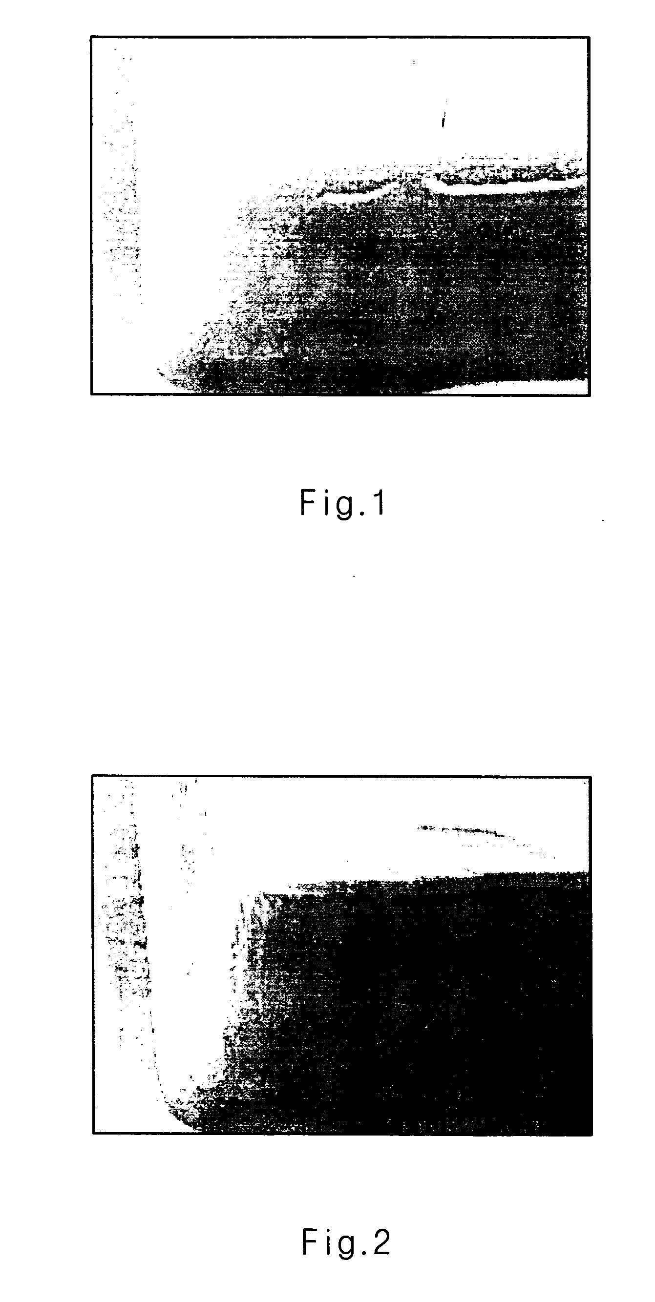
Figure 1 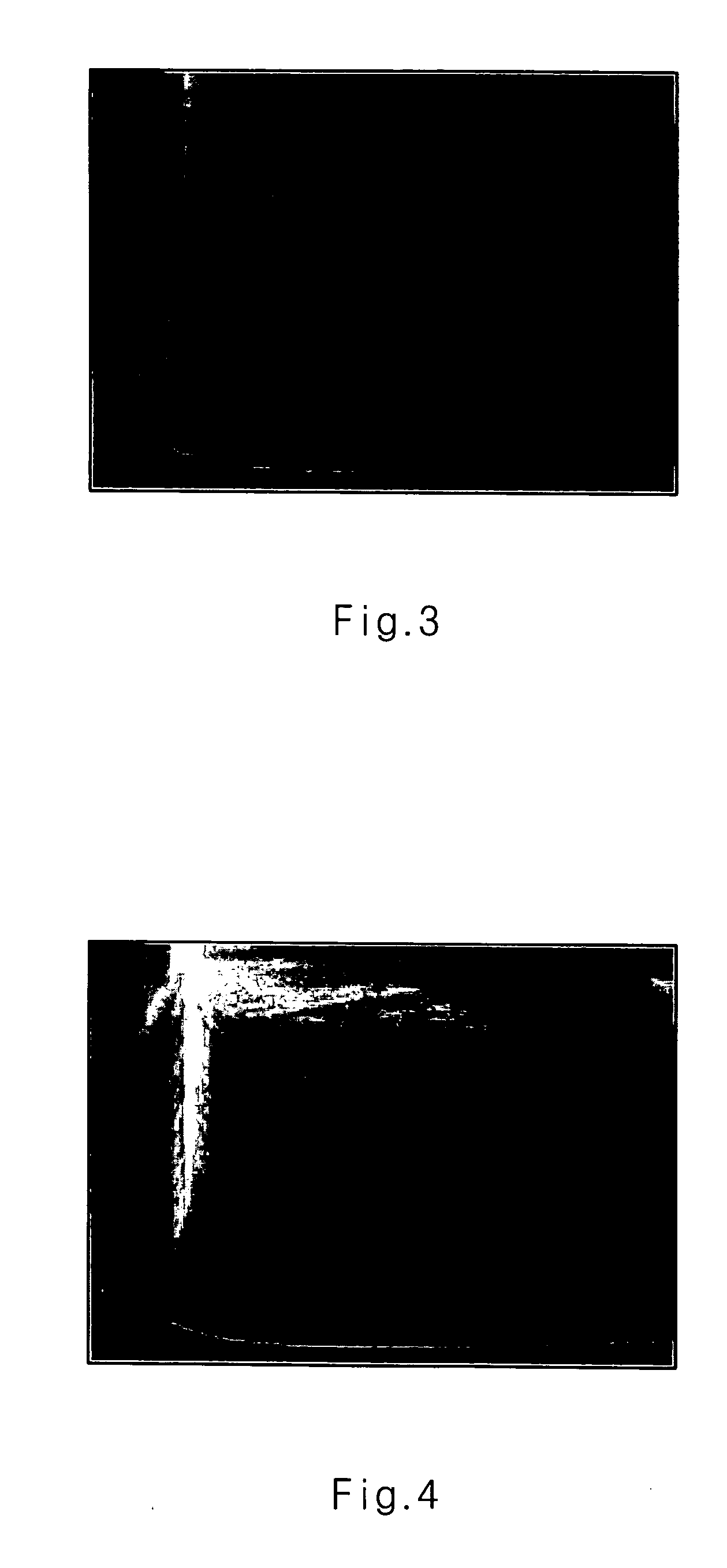
Figure 2 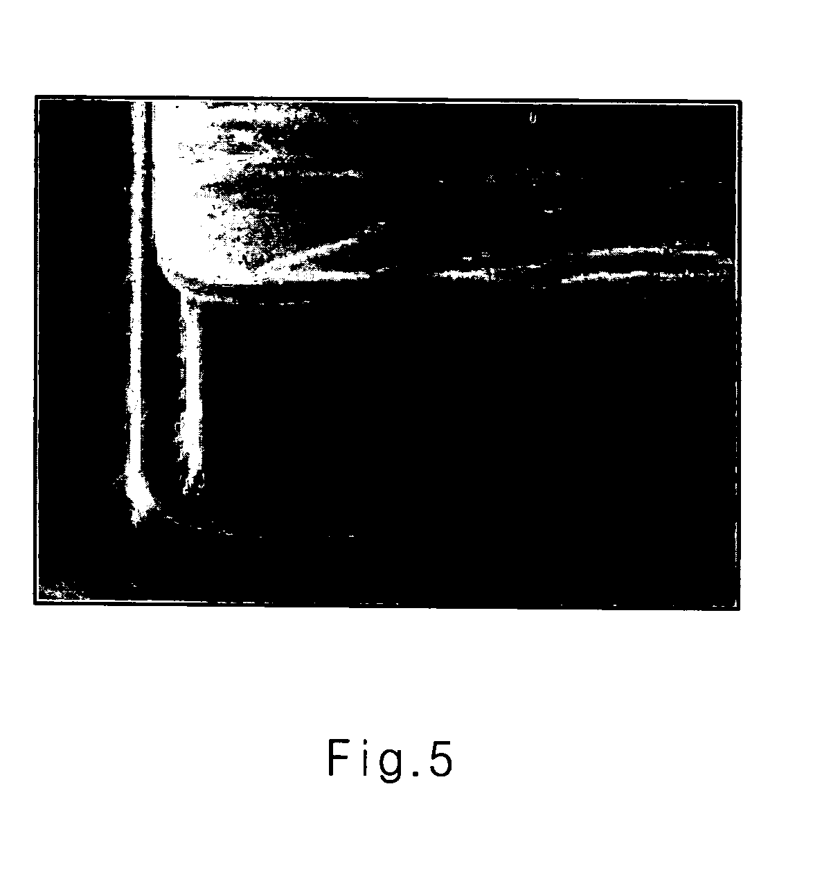
Figure 3
Abstract
Description
[0001] Methods of manufacturing semiconductor devices using a photoresist polymer remover composition are disclosed. The photoresist polymer remover composition effectively removes photoresist residuals generated from etching or ashing sub-processes in photoresist pattern forming processes during the manufacturing of semiconductor devices.DESCRIPTION OF THE RELATED ART
[0002] In a conventional semiconductor device manufacturing process, a photoresist pattern is formed on a conductive layer which has been formed on a semiconductor substrate. The conductive layer whose portion is not covered by the pattern is etched using the photoresist pattern as a mask to form a conductive layer pattern. This lithography process is then repeated to form the conductive patterns
[0003] The photoresist pattern is used as the mask and it should be removed from the conductive layer with a photoresist remover in a strip process after the process for forming the conductive layer pattern is completed. Howeve...
Examples
experimental example 1
Removal of Polymer
(1) Preparation of Test sample A
[0045] On an 8-inch silicon wafer where a titanium nitride film, an aluminum film and a titanium film were sequentially deposited from the lower to the upper portion at 100 .ANG., 8000 .ANG. and 400 .ANG., respectively, a conventional positive-type resist composition sold under the designation "DPR-i1000" by Dongjin Semichem Co. Ltd. was spin-coated to obtain a resist film of 1.01 .mu.m. Thereafter, the resist film was pre-baked on a hot plate at 110.degree. C. for 90 seconds. A mask having a predetermined pattern was located on the resist film, and irradiated with ultraviolet rays. Then, the exposed resist film was developed at 21.degree. C. for 60 seconds by TMAH developing solution of 2.38 wt % to form a photoresist pattern. A test sample where the photoresist pattern was formed was hard-baked at 120.degree. C. for 100 seconds on the hot plate. The titanium nitride film, the aluminum film and the titanium film were etched using th...
experimental example 2
(1) Preparation of Test sample B
[0049] The procedure of Example 1 was repeated to obtain Test sample B.
(2) Experiment of Metal Film Corrosion
[0050] The Test sample B was soaked in each photoresist polymer remover composition of Examples 1-5 and Comparative Examples 1-3 at room temperature. The Test sample B was washed with ultra pure water and dehydrated with nitrogen gas. Then, whether an undercut phenomenon occurred in the lower metal film was examined by SEM to show corrosion degree of the lower metal film.
3 TABLE 3 Soaking Time 1 min. 3 min. 5 min. Example 1 .largecircle. .largecircle. .largecircle. 2 .largecircle. .largecircle. .largecircle. 3 .largecircle. .largecircle. .largecircle. 4 .largecircle. .largecircle. .largecircle. 5 .largecircle. .largecircle. .largecircle. Comparative 1 X X X Example 2 .largecircle. .largecircle. .largecircle. 3 .largecircle. .largecircle. .largecircle. .largecircle.: when the undercut phenomenon did not occur in the lower ...
experimental example 3
Application to Production Line
[0053] The evaluation results of a disclosed remover composition applied to semiconductor device production line are shown in the following tables 4 (hole pattern forming process) and 5 (line pattern forming process).
4TABLE 4 Device / Process Evaluation Item Evaluation Result 64MSD G / Process1 Polymer removability Completely removed Post-Cleaning Sidewall film (HSQ) attack None Titanium nitride film attack None Foreign substance test on run No specific foreign substance, (KLA foreign substance test) No plug missing PT1(Probe Test) / PCM(Process No significant difference Control Monitoring Test) compared to the conventional remover WFBM(Wafer Fail Bit Map) .fwdarw. No related fail M2C related fail PKG Test No significant difference compared to the conventional remover 256M DDR(BC) / Process1 Polymer removability Completely removed Post-cleaning Sidewall film (HSQ) attack None Titanium nitride film attack None Foreign substance test on run No specific foreign su...