
Resistive memory device and operation method thereof
Patent Information
- Authority / Receiving Office
- US · United States
- Current Assignee / Owner
- Publication Date
- 2019-05-30
Smart Images
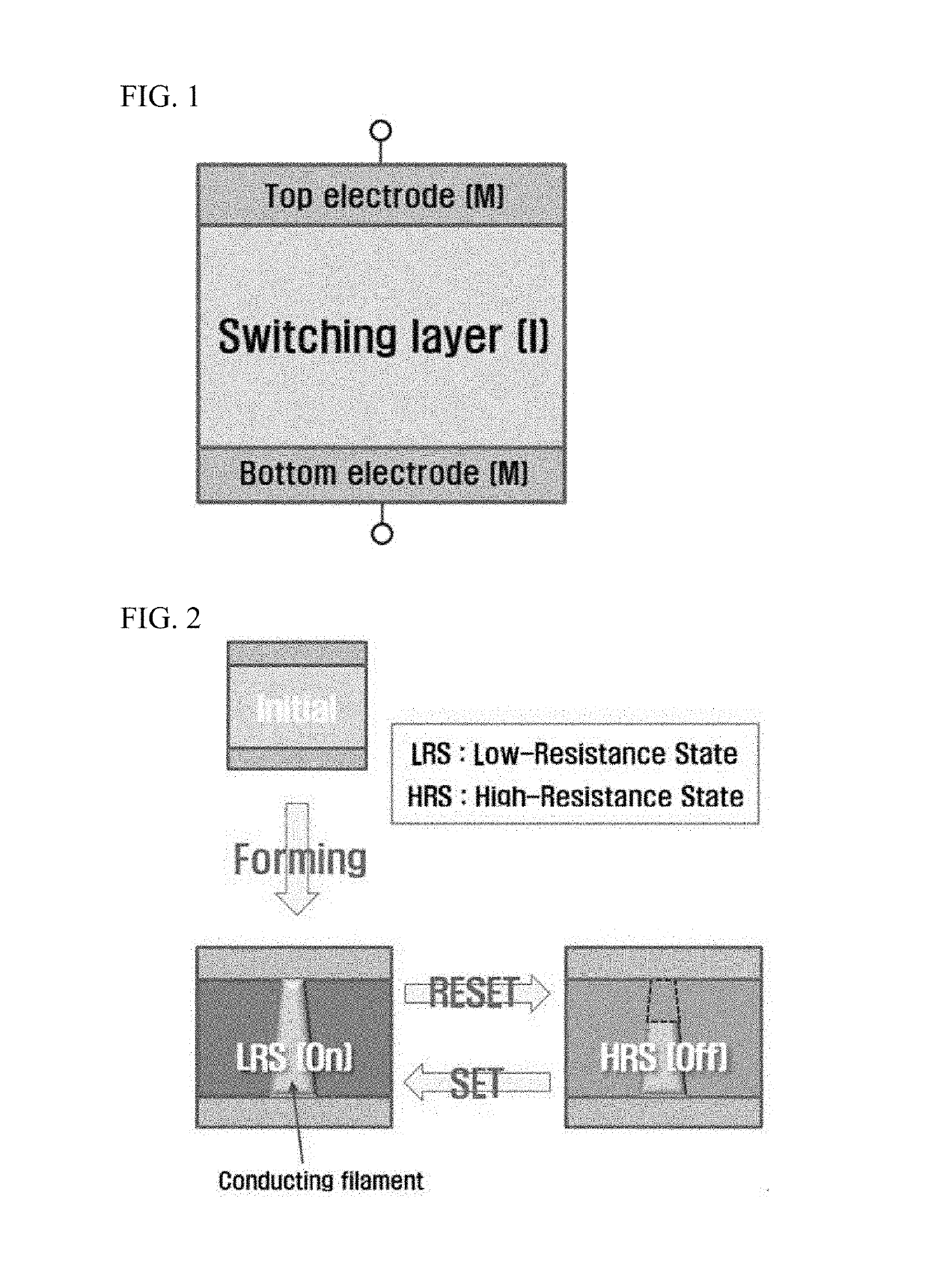
Figure 1 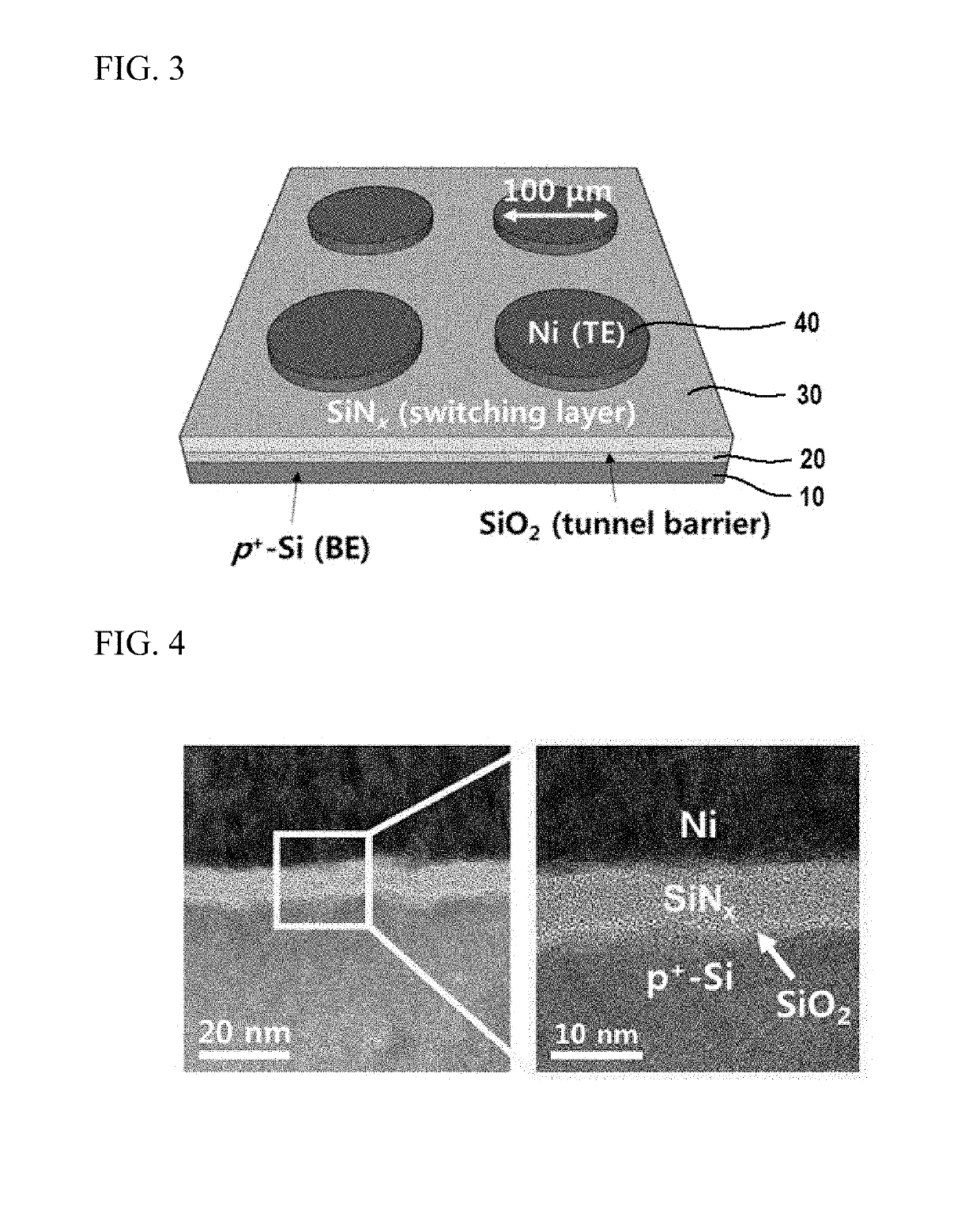
Figure 2 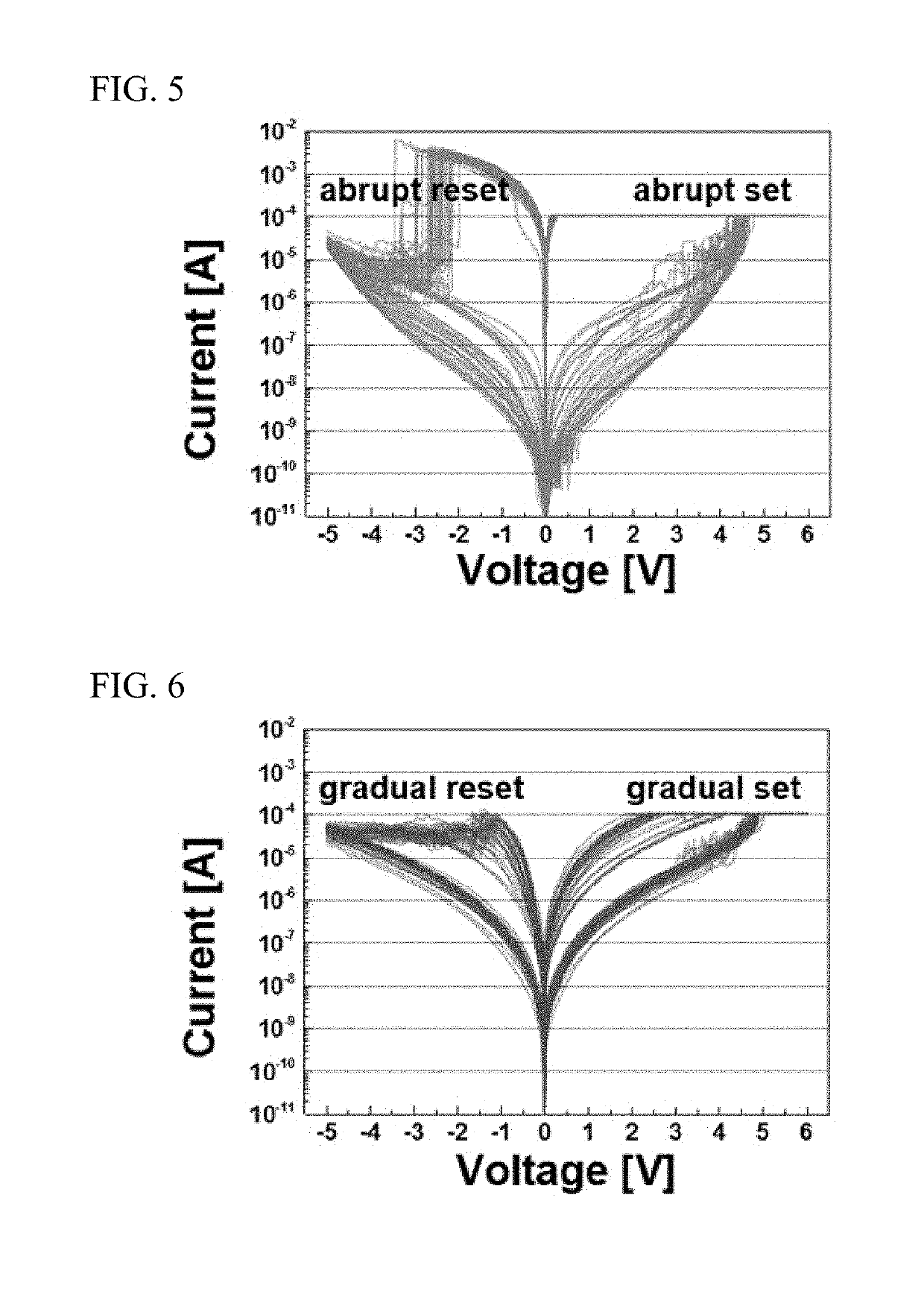
Figure 3
Abstract
Description
CROSS-REFERENCE TO RELATED APPLICATION
[0001] This application claims priority to Korean Patent Application No. 10-2017-0161384, filed on Nov. 29, 2017, under 35 U.S.C. 119, the entire contents of which are hereby incorporated by reference.BACKGROUNDField of the Invention
[0002] The present invention relates to a resistive memory device, and more particularly to a resistance change memory device, in which the conductance is changed symmetrically in a SET operation and a RESET operation, and a method of operation thereof. The resistive memory device of the present invention is used for efficient and accurate data storage as a RRAM (Resistive Random Access Memory) in a high-capacity memory array, and as a synaptic device in a neuromorphic system.
[0003] NAND flash memory technology is currently leading the mass storage market through continuously scaling down. However, in recent years, as the size of the device has been reduced to 20 nm or less, several reliability problems have arisen. The...
Examples
Embodiment Construction
[0029]Detailed descriptions of preferred embodiments of the present invention are provided below with accompanying drawings.
[0030]As exemplary shown in FIG. 3, a resistive memory device according to an embodiment of the present invention comprises a bottom electrode 10 formed by doping impurities into a semiconductor material; a resistance change layer 20 or / and 30 formed on the bottom electrode; and a top electrode 40 formed on the resistance change layer, wherein the resistance change layer comprises an oxide film 20 formed on the bottom electrode 10 and a nitride film 30 formed on the oxide film 20.
[0031]The semiconductor material may be other materials such as germanium but may be silicon. In the latter case, it may be crystalline silicon or polycrystalline silicon. Therefore, the bottom electrode 10 may be p+-Si doped with a high concentration of p-type impurities (for example, 5×10¹⁵ / cm2) into silicon as shown in FIG. 3.
[0032]The oxide film 20 may be formed of any material if ...