Electric power circuit, display driver and voltage supply method

A technology of power supply circuit and voltage supply, applied in static indicators, instruments, adjusting electrical variables, etc., can solve problems such as the enlargement of the switching circuit scale and the increase of the on-resistance R loss of the MOS transistor, and achieve the best image quality reduction. The effect of lowering, lowering power consumption, and reducing self-consumption power

Inactive Publication Date: 2007-11-21
SEIKO EPSON CORP
View PDF5 Cites 2 Cited by
  • Summary
  • Abstract
  • Description
  • Claims
  • Application Information

AI Technical Summary

Problems solved by technology

In this case, the resistance R can be reduced by increasing the channel width W of the MOS transistor, but the scale of the switching circuit will become larger
And, the loss of the on-resistance R of the MOS transistor will also increase

Method used


Image

  • Electric power circuit, display driver and voltage supply method
  • Electric power circuit, display driver and voltage supply method
  • Electric power circuit, display driver and voltage supply method

Examples


Embodiment Construction

[0055] Hereinafter, embodiments of the present invention will be described in detail with reference to the drawings. In addition, the embodiment described below does not unduly limit the content of the present invention described in the claims. Furthermore, not all components described below are necessarily essential components of the present invention.

[0056] 1. Liquid crystal display device

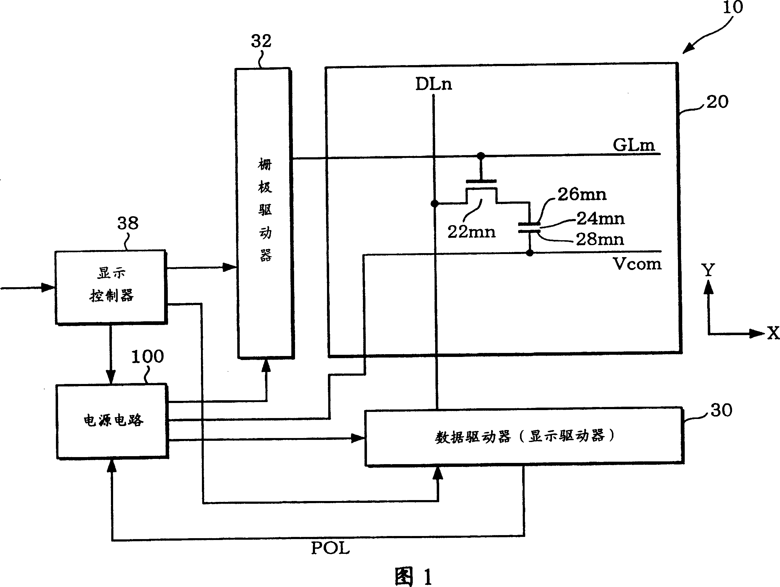
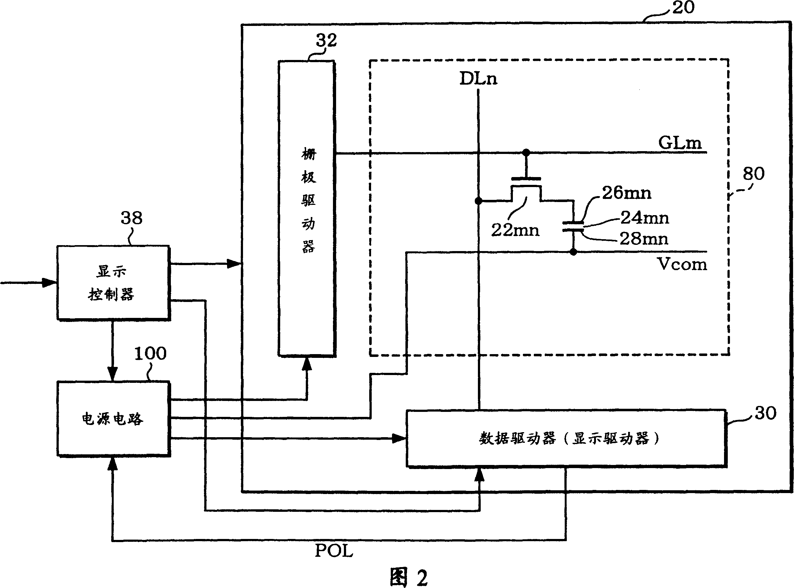
[0057] FIG. 1 shows an outline of the composition of an active matrix type liquid crystal display device including a power supply circuit according to this embodiment.

[0058] The liquid crystal display device 10 includes a liquid crystal display panel (in a broad sense, a display panel) 20 .

[0059] The liquid crystal display panel 20 is, for example, formed on a glass substrate. The glass substrate is configured with: scanning lines (gate lines) GL1-GLM (M is an integer greater than or equal to 2), a plurality of scanning lines are arranged in the Y direction, and extend to the...


PUM


Abstract

A power supply circuit. When the voltage is to be supplied to a counter electrode opposing a pixel electrode via an electro-optic substance by switching from a first voltage VCOML in the lower potential side to a first voltage VCOMH in the high potential side, a second voltage VCOMH1 in the high potential side at a higher potential than the first voltage VCOMH is first supplied to the counter electrode instead of the first voltage VCOML in the lower potential side, and then the first voltage VCOMH in the high potential side is supplied. Or, prior to supplying the second voltage VCOMH1 in the high potential side to the counter electrode, either the first voltage VCOMH in the high potential side or a first intermediate voltage VCOMH2 at a lower potential than the first voltage VCOMH in the high potential side but at a higher potential than the first voltage VCOML in the lower potential side may be supplied to the counter electrode.

Description

technical field [0001] The invention relates to a power supply circuit, a display driver and a voltage supply method. Background technique [0002] An active matrix type liquid crystal display device includes a plurality of scanning lines and a plurality of data lines formed in a matrix shape. Moreover, it also includes: a plurality of switching elements, wherein each switching element is connected to each scanning line and each data line; a plurality of pixel electrodes, wherein each pixel electrode is connected to each switching element. The pixel electrode is opposed to the counter electrode through a liquid crystal (electro-optical substance in a broad sense). [0003] In the liquid crystal display device having such a structure, the voltage supplied from the data line is applied to the pixel electrode through the switching element turned on by the selected scanning line. And, the transmittance of the pixel varies according to the voltage applied between the pixel elec...

Claims


Application Information

Patent Timeline
Patent Type & Authority Patents(China)
IPC IPC(8): G09G3/20G09G3/36G02F1/133G05F1/40
CPCG09G3/3655G09G3/3696
Inventor 森田晶
Owner SEIKO EPSON CORP
Why Eureka
Try Eureka