Dynamic self-management buffer zone

A buffer device and self-management technology, applied in the direction of input/output to the record carrier, etc., can solve the problems of waste of logic resources, poor scalability, occupation, etc., and achieve the effect of simplifying logic design, avoiding waste of space, and convenient for expansion

Inactive Publication Date: 2008-06-18
HUAWEI TECH CO LTD
View PDF3 Cites 0 Cited by
  • Summary
  • Abstract
  • Description
  • Claims
  • Application Information

AI Technical Summary

Problems solved by technology

[0008] 2. Waste of logical resources: The buffer is generally implemented by an embedded storage block (ESB) inside the logic. The size of each ESB is fixed. At least one ESB is required to construct a physical bank. Even if all ESB resources are not used, one bank occupies one ESB. , so that the actual utilization of the ESB is low
[0009] 3. Poor scalability: If you want to expand the number of BANKs, the management complexity will be greatly increased: As mentioned earlier, this kind of buffer requires each BANK to correspond to a physical ESB entity, so there will be independent control buses, data Bus, so that each additional BANK will introduce an additional set of buses, which will lead to more complex buffer management and further waste of logic resources

Method used


Image

  • Dynamic self-management buffer zone
  • Dynamic self-management buffer zone
  • Dynamic self-management buffer zone

Examples


Embodiment Construction

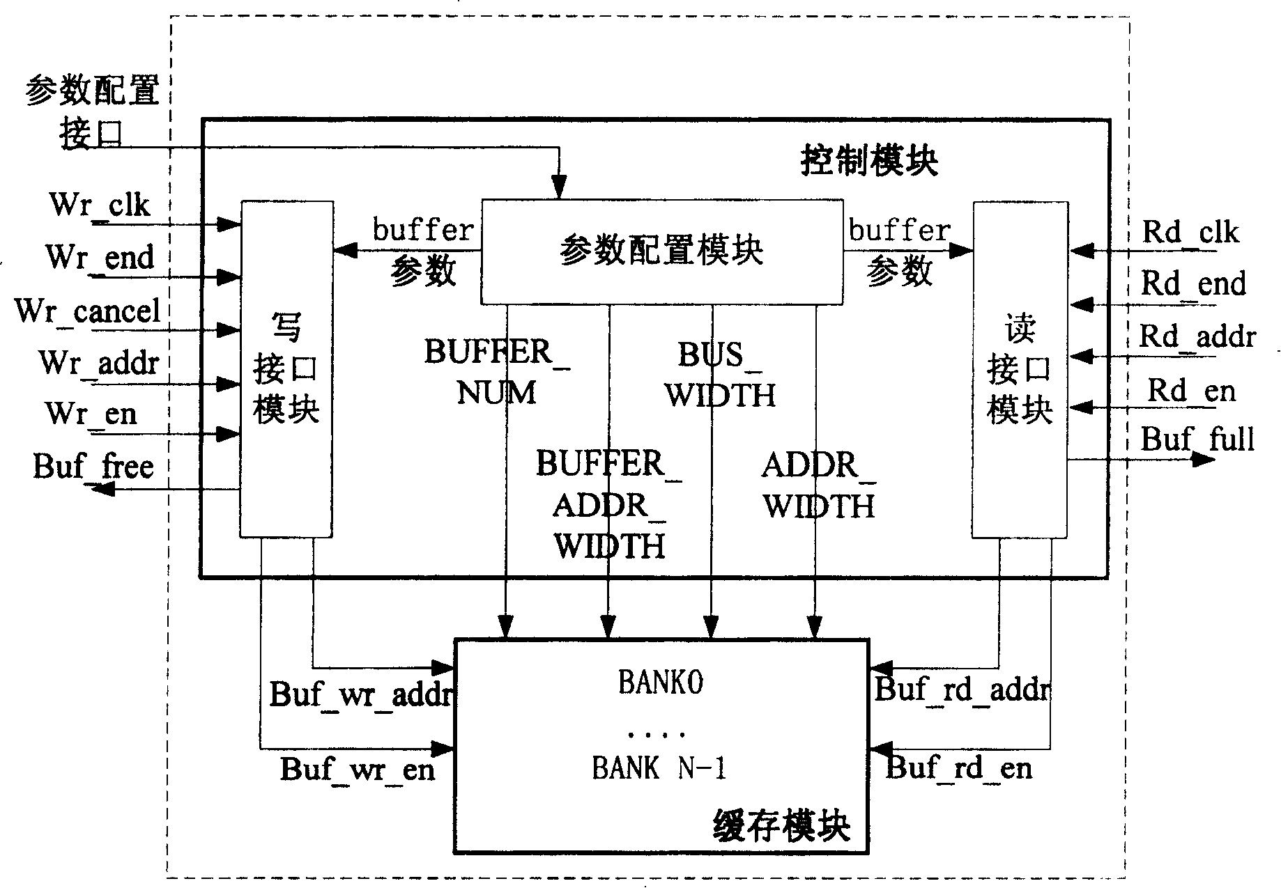
[0026] The invention provides a new buffer. The buffer provides a unified interface to the external modules. The operator does not need to care about the internal BANK structure of the buffer, and all bank switching is managed by the buffer itself.

[0027] Such as image 3 The buffer structure diagram of the present invention shown includes a control module (Control Module) and a cache module (Buffer). The cache module is internally divided into multiple BANKs; the control module controls the reading and writing of BANKs, as well as the configuration of BANKs inside the cache module. The control module further includes a write interface module, a read interface module, and a parameter configuration module. The internal management of all buffers is uniformly controlled by the control module, including realizing BANK parameter configuration, BANK empty and full flag generation, BANK automatic switching, BANK reading and writing, etc. Detailed description will be given below. ...


PUM


Abstract

The present invention includes control module and cache module, wherein said cache module divided into plurality of BANK spaces; control module used for receiving outer read-write signal, controlling data writing / reading out cache module every BANK, and configuring inner BANK of cache module. Said control module also includes writing interface module, interface module, parameter configuring module, wherein writing interface module used for receiving outer write data signal and controlling data writing cache module BANK; read interface module used for receiving outer read data signal, controlling data reading out cache module BANK; parameter configuring module used for transferring configuration parameter to cache module to proceed configuring and transferring configuration parameter to writing interface module and read interface module. The present invention can simplify outside managing to buffer zone, and to make the external interface not concerning buffer zone inner BANK structure.

Description

technical field [0001] The invention relates to the technical field of buffers, in particular to a dynamic self-management buffering device. Background technique [0002] In hardware design, programmable logic devices (FPGA) are often used to complete various algorithm processing, complex interface timing conversion, and so on. However, inside the FPGA, when data is transmitted between different functional sub-modules (or logic units), cross-clock domain problems may occur, resulting in data transmission failure. For example, the logic interface module inside the FPGA is inconsistent with the processing clock of the internal module, which will cause data to fail to be transmitted normally between the two logic units. [0003] At present, buffer isolation is usually used to solve the problem of crossing clock domains, and the buffer can be implemented by FIFO or DPRAM. Among them, FIFO has the address self-increment function, so there is no need to provide an address line e...

Claims


Application Information

Patent Timeline
Patent Type & Authority Patents(China)
IPC IPC(8): G06F3/06
Inventor 段勇
Owner HUAWEI TECH CO LTD
Why Eureka
Try Eureka