
Electronic tap connecting element, assembly and insulation cover thereof
A technology for connecting components and electronics, applied in the manufacturing of electrical components, connections, contacts, etc., can solve the problems of uneven force, reduced reliability of U-shaped connecting terminals 22, etc., to increase the service life and increase the current transmission capacity. Effect
Patent Information
- Authority / Receiving Office
- CN · China
- Patent Type
- Applications(China)
- Current Assignee / Owner
- Publication Date
- 2007-09-19
- Estimated Expiration
- Not applicable · inactive patent
Smart Images
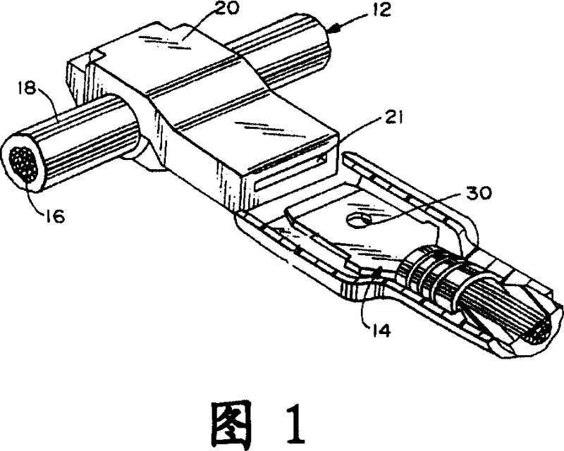
Figure 1 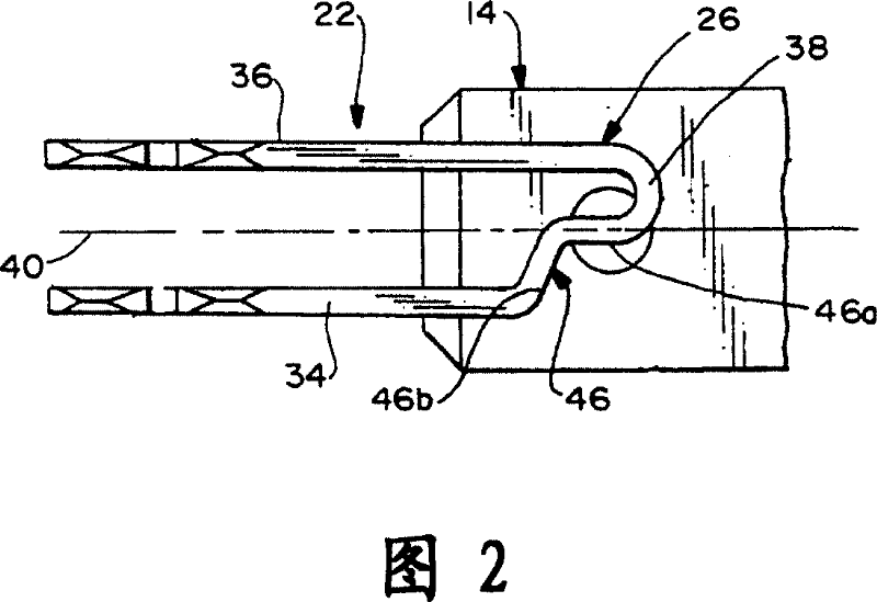
Figure 2 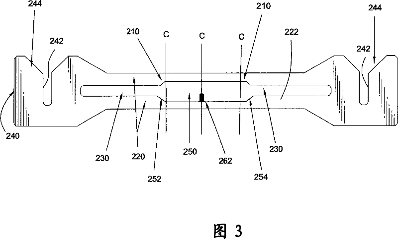
Figure 3
Abstract
Description
technical field
[0001] The present invention relates to an electronic tap connection component, in particular to an electronic tap connection component formed by stamping, having a wire receiving portion at one end and a sheet receiving portion at the other end share. Background technique
[0002] In the modern digital age, it is necessary to connect various devices or signals or power sources together to make the system function, which requires many connecting elements to connect them in series. There are many electronic connection terminals designed to receive or mate with one or blade contacts. Such connecting terminals are usually used on tap connectors to form T-shaped connections with insulated wires. In this type of connection terminal, it must provide a wire receiving part including an insulation displacement (InsulationDisplacement Terminal, IDT) at one end, and a matable sheet receiving part at the other end. Based on the requirements of these two connections, t...
Examples
Embodiment Construction
[0037] Since the present invention discloses a structure of an electronic tap connection component, the connection terminals formed by some stamping process technologies used therein and the combination of the connection terminals and the insulating housing (housing) have been disclosed in detail in the prior art , so in the following description, the related stamping process of the connection terminal and the combination process of the connection terminal and the insulating cover are not fully described. Moreover, the drawings in the following texts are not completely drawn according to the actual relevant dimensions, and their function is only to express the schematic diagrams related to the features of the present invention.
[0038] First of all, please refer to FIG. 3 , which is a thin metal plate structure produced by the stamping process of the present invention. The thin metal plate will form a similar W-shaped terminal 200 structure after proper processing. The thin m...