

A method of performing model-based scanner tuning
A scanner and imaging model technology, which can be used in instruments, photolithography process of pattern surface, microlithography exposure equipment, etc., can solve the problems of time-consuming, expensive, and achieve low-cost
- Summary
- Abstract
- Description
- Claims
- Application Information
AI Technical Summary
Problems solved by technology
Method used
Image

Examples
Embodiment Construction
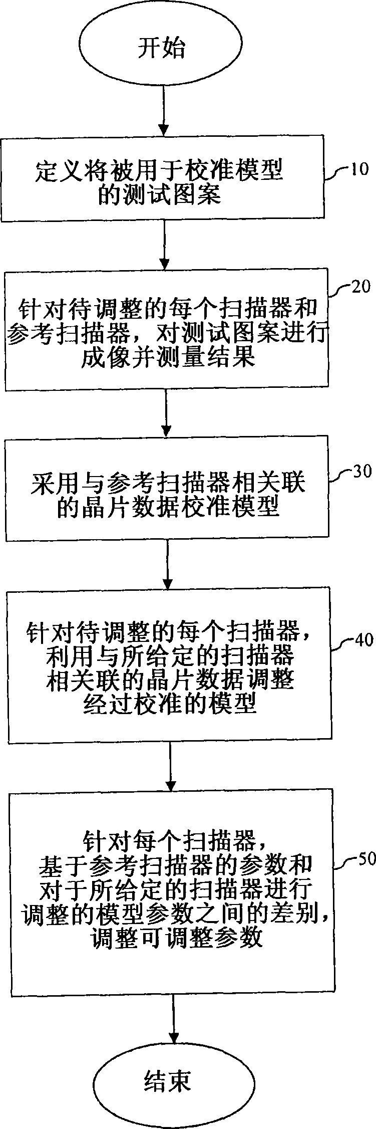
[0031] figure 1 is an exemplary flowchart representing the model-based scanner tuning method of the present invention. As explained in detail below, the method of the present invention allows simultaneous optimization of imaging performance and OPE matching between different lithographic systems comprising scanners for imaging the same target pattern .
[0032] refer to figure 1 , the first step in the process (step 10) is to define a test pattern for calibrating the model of the reference scanner. Suitable test patterns (also known as phantom calibration metric patterns) can be used. The test pattern employed should sufficiently represent the features to be imaged so that it is possible to generate a robust model capable of accurately predicting the imaging performance of the lithography system. Such test patterns can be easily generated / selected by one skilled in the art once the target pattern or application is determined. It should be noted that it is also possible to...
PUM
 Abstract
Description
Claims
Application Information