Eureka AIR delivers breakthrough ideas for toughest innovation challenges, trusted by R&D personnel around the world.

Tin-lead recovery method in waste circuit board

A waste circuit board, recycling method technology, applied in the field of heavy metal recycling by chemical method, can solve the problems of restriction, waste of tin and lead resources, etc., and achieve the effect of preventing pollution, improving environmental quality, high economic benefit and environmental significance

Inactive Publication Date: 2011-06-01
刘景洋
View PDF0 Cites 3 Cited by
  • Summary
  • Abstract
  • Description
  • Claims
  • Application Information

AI Technical Summary

Problems solved by technology

[0003] The traditional process of dismantling components with acid-soluble solder is limited due to the generation of a large amount of waste acid
In the traditional treatment method, after the acid dissolves the solder to disassemble the electronic components, the tin and lead in the solution are removed by precipitation, and the precipitation is then sent to the hazardous waste treatment site as hazardous waste for landfill, resulting in a waste of tin and lead resources

Method used


Image

  • Tin-lead recovery method in waste circuit board
  • Tin-lead recovery method in waste circuit board
  • Tin-lead recovery method in waste circuit board

Examples


Embodiment 1

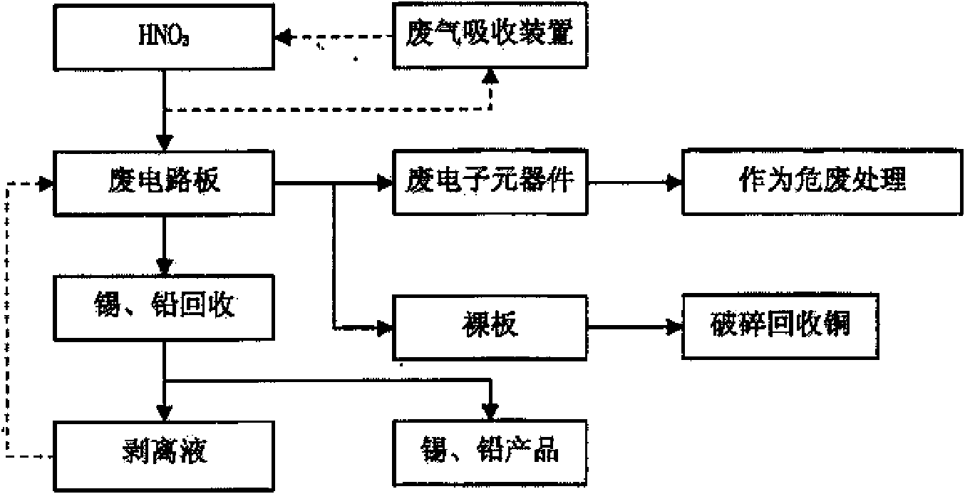
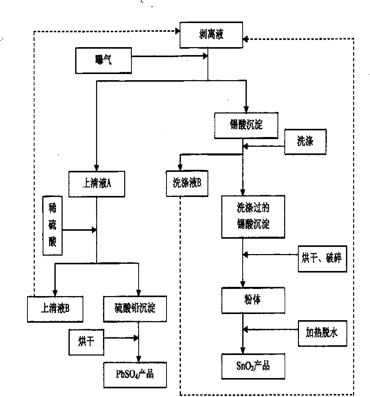
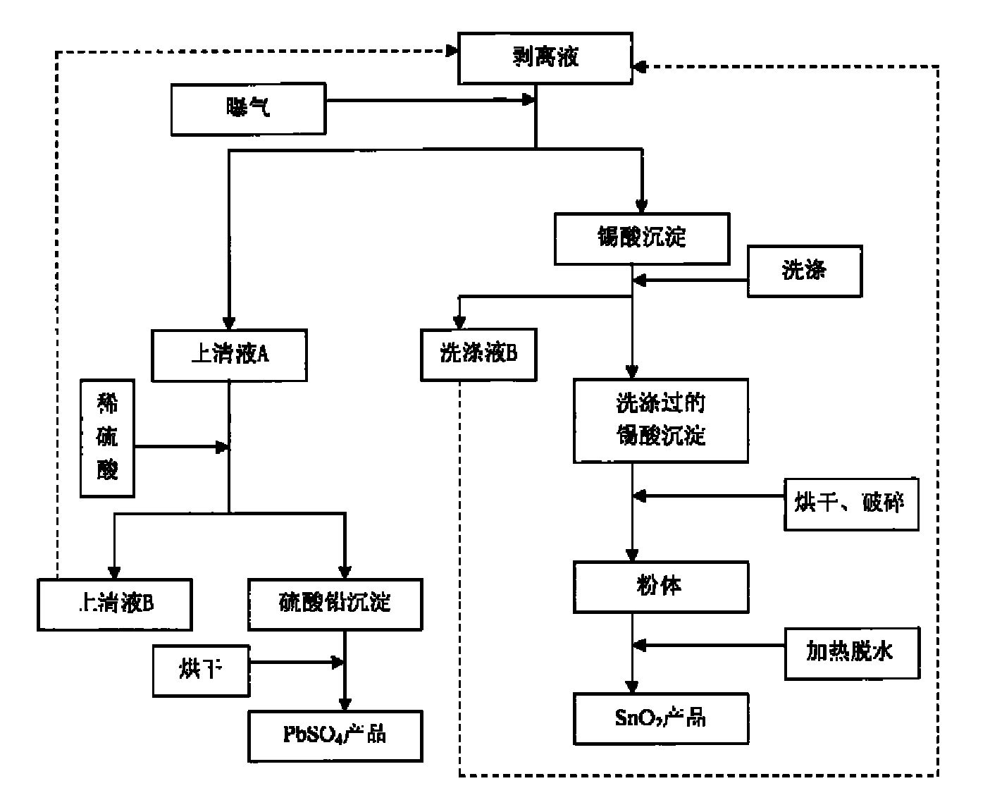
[0026] A method for recovering tin and lead in waste circuit boards, the method is to first wet strip the electronic components on the waste circuit boards, then carry out the classification precipitation and recovery of tin and lead in the waste circuit boards, and reclaim the The waste gas and waste liquid generated in the process are reused in the recovery process;

[0027] The method sequentially includes the following steps:

[0028] I. Dismantling of electronic components:

[0029] A. Use HNO to waste circuit boards 3 Carry out soaking treatment; Described soaking treatment time is 6 hours, and described HNO 3 The concentration of the waste circuit board is 1mol / L; after the electronic components of the waste circuit board fall off, the bare board, the waste electronic components, and the primary stripping liquid are obtained; the primary stripping liquid is filtered to obtain the stripping liquid; the Filtration treatment adopts filter cloth;

[0030] B. Wash the ba...

Embodiment 2

[0045] The steps of the method for recycling tin and lead in waste circuit boards described in this embodiment are the same as those in Embodiment 1, the difference being:

[0046] I. Dismantling of electronic components:

[0047] A. Use HNO to waste circuit boards 3Carry out soaking treatment; Described soaking treatment time is 4 hours, and described HNO 3 The concentration is 2mol / L;

[0048] After testing, the SnO 2 The product has a purity of 99%, the PbSO 4 The purity of the product reaches 99%; the recovery rate of tin and lead in the waste circuit board reaches 99%; the detection method is the same as in Example 1.

Embodiment 3

[0050] The steps of the method for recycling tin and lead in waste circuit boards described in this embodiment are the same as those in Embodiment 1, the difference being:

[0051] I. Dismantling of electronic components:

[0052] A. Use HNO to waste circuit boards 3 Carry out soaking treatment; Described soaking treatment time is 1 hour, and described HNO 3 The concentration is 3mol / L;

[0053] After testing, the SnO 2 The product has a purity of 90%, the PbSO 4 The purity of the product reaches 90%; the recovery rate of tin and lead in the waste circuit board reaches 98%; the detection method is the same as in Example 1.


PUM


Abstract

The invention provides a tin-lead recovery method in a waste circuit board. The method comprises the following steps of: wet-stripping electronic components on a waste circuit board, carrying out classified deposition and recovery of tin and lead in the waste circuit board, and reusing waste gas and waste liquid generated in the recovery process into the recovery process. The method can effectively prevent the pollution of waste acid, waste gas and waste metal generated in the recovery process of the waste circuit board, improve environment quality of a centralized recovery area and reduce the cost of pollution control in the recovery process.

Description

technical field [0001] The invention belongs to the field of recovering heavy metals by chemical methods, and in particular relates to a method for recovering tin and lead in waste circuit boards; the method is to firstly peel off the electronic components on the waste circuit boards by wet method, and then carry out the described tin-lead recovery method in the waste circuit boards. 1. The classified precipitation and recovery of lead, and the waste gas and waste liquid generated in the recovery process are reused in the recovery process. Background technique [0002] The output of printed circuit board (PCB) in mainland China ranks first in the world, accounting for 26% of the world's total output, and is developing at an annual growth rate of about 15%. Correspondingly, the annual production of major electronic waste in my country is 1.5 million tons, and it is growing at a rate of 13% to 15% per year, which is three times that of ordinary domestic waste. Due to the high...

Claims


Application Information

Patent Timeline
Patent Type & Authority Patents(China)
IPC IPC(8): C22B7/00C22B25/06C22B13/00C23F1/30
Inventor 刘景洋郭玉文乔琦
Owner 刘景洋
Why Eureka
Eureka Blog
Learn More