

Method for manufacturing front panel of plasma display screen
A technology of a plasma display screen and a manufacturing method, which is applied in the field of manufacturing a front panel of a plasma display screen, can solve the problems of poor display quality, large alignment deviation, poor picture quality, etc., and achieves improved display quality, reduced alignment deviation, The effect of improving yield
- Summary
- Abstract
- Description
- Claims
- Application Information
AI Technical Summary
Problems solved by technology
Method used
Image

Examples
Embodiment Construction
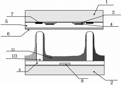
[0024] Such as figure 1 As shown, the plasma display adopts a three-electrode surface discharge structure, including a front panel 1 and a rear panel 2 sealed together with it. The front panel 1 is provided with ITO electrodes 3 and BUS electrodes 4, which form a discharge The display electrode of the present invention has a transparent dielectric layer 5 made on the electrode surface, and a MgO layer 6 is vapor-deposited on the transparent dielectric layer 5 . There are black stripes 7 in the direct non-luminous area of the display electrodes. ADD electrodes 8 perpendicular to the display electrodes are arranged on the rear panel 2, and the ADD electrodes 8 are covered with a rear dielectric layer 9, on which a barrier rib pattern 10 is formed, and a phosphor layer 11 is printed in the barrier rib groove. After the front panel 1 and the rear panel 2 are combined, they are sealed together by low-melting glass powder, and the display screen is filled with working gas Xe+Ne. ...
PUM
| Property | Measurement | Unit |
|---|---|---|
| thickness | aaaaa | aaaaa |
| thickness | aaaaa | aaaaa |
| thickness | aaaaa | aaaaa |
Abstract
Description
Claims
Application Information