

Multilayer circuit board method with high density interconnection and high reliability combination
A high-density interconnection, multi-layer circuit board technology, applied in the direction of multi-layer circuit manufacturing, etc., can solve the problems of large resistance change rate of circuit boards and various failures of circuit board products.
- Summary
- Abstract
- Description
- Claims
- Application Information
AI Technical Summary
Problems solved by technology
Method used
Image

Examples
Embodiment Construction
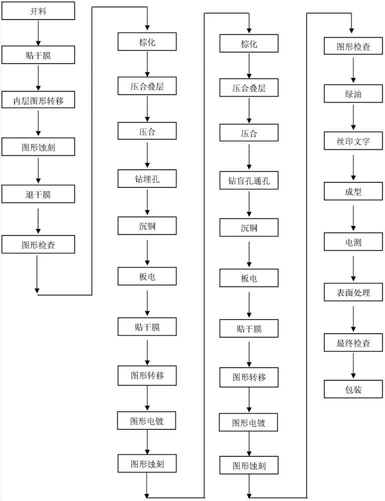
[0040] A method for manufacturing a multilayer circuit board combined with high-density interconnection and high reliability, comprising the steps of:
[0041] Step 1: Cutting the material, and cutting out the circuit board surface that meets the design requirements;
[0042] Step 2: Paste the dry film, and paste the dry film on each layer of the inner layer;
[0043] Step 3: transfer the graphics on the inner layer, using film exposure technology to transfer the graphics on the inner layer to the board;
[0044] Step 4: Graphic etching, use etching potion to etch away all unnecessary positions, and keep the required positions.
[0045] Step 5: Remove the dry film, remove all the pasted dry film, and expose the copper surface and the circuit;
[0046] Step 6: Graphic inspection, use a scanning instrument to check out the open and short circuit defects of the circuit;
[0047] Step 7: Browning, roughening the copper surface and wire surface of each layer of the inner layer, ...
PUM
 Abstract
Description
Claims
Application Information