

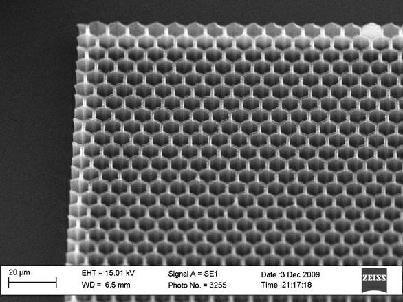
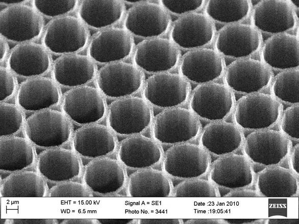
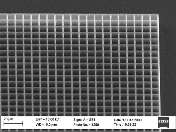
Orientated-growth latticed high-performance carbon nano-tube field emission array
A carbon nanotube array and carbon nanotube technology, which is applied to the components of discharge tubes/lamps, electrical components, circuits, etc., can solve the problems of carbon nanotube orientation deterioration and area waste, and reduce the opening electric field and threshold Effects of electric fields, improved structural stability, enhanced edge effects
- Summary
- Abstract
- Description
- Claims
- Application Information
AI Technical Summary
Problems solved by technology
Method used
Image

Examples
Embodiment
[0020] Embodiment, the preparation process of the high-performance grid-mounted carbon nanotube array is as follows:
[0021] (1) First, select a heavily doped silicon wafer as the substrate, wash the silicon wafer in acetone (acetone) and isopropanol (IPA) for two minutes to remove surface organic matter and other impurities, bake to 180°C and keep Two minutes to remove moisture from the surface.
[0022] (2) Then spin-coat a layer of electron beam photoresist on the surface, and harden the film at a temperature of 180°C for 90 seconds.
[0023] (3) The photoresist is photoetched to form a grid pattern, and after development, a photoresist mask with a pattern is prepared.
[0024] (4) Then sputter a catalyst film on the surface of the sample by magnetron sputtering. The catalyst here is composed of two layers of films, the lower layer is an Al film with a thickness of 10nm, and the upper layer is a Fe film with a thickness of 1nm.
[0025] (5) Stripping, the sample is immer...
PUM
| Property | Measurement | Unit |
|---|---|---|
| thickness | aaaaa | aaaaa |
| thickness | aaaaa | aaaaa |
Abstract
Description
Claims
Application Information