Pixel circuit, driving method thereof and display device

A pixel circuit and driving method technology, applied in the display field, can solve problems such as non-uniformity, difference, and change, and achieve the effects of slowing down the decay rate, increasing service life, and improving uniformity

Active Publication Date: 2013-09-18
BOE TECH GRP CO LTD
View PDF5 Cites 37 Cited by
  • Summary
  • Abstract
  • Description
  • Claims
  • Application Information

AI Technical Summary

Problems solved by technology

[0003] In the existing AMOLED display panel, each OLED includes a plurality of TFT (Thin Film Transistor, thin film transistor) switch circuits. Due to the limitation of production process and production level, etc., the TFT switch circuits fabricated on a large-area glass substrate Non-uniformity often occurs in electrical parameters such as threshold voltage and mobility, so that the current flowing through the AMOLED will not only change with the change of the on-voltage stress generated by the long-time conduction of the TFT, but also with the TFT threshold voltage drift varies with
In this way, it will affect the brightness uniformity and brightness constancy of the display
On the other hand, the AMOLED in the working state will also be in the bias state for a long time, which accelerates the decay rate of the display device, thereby reducing the life of the display device

Method used


Image

  • Pixel circuit, driving method thereof and display device
  • Pixel circuit, driving method thereof and display device
  • Pixel circuit, driving method thereof and display device

Examples


Embodiment Construction

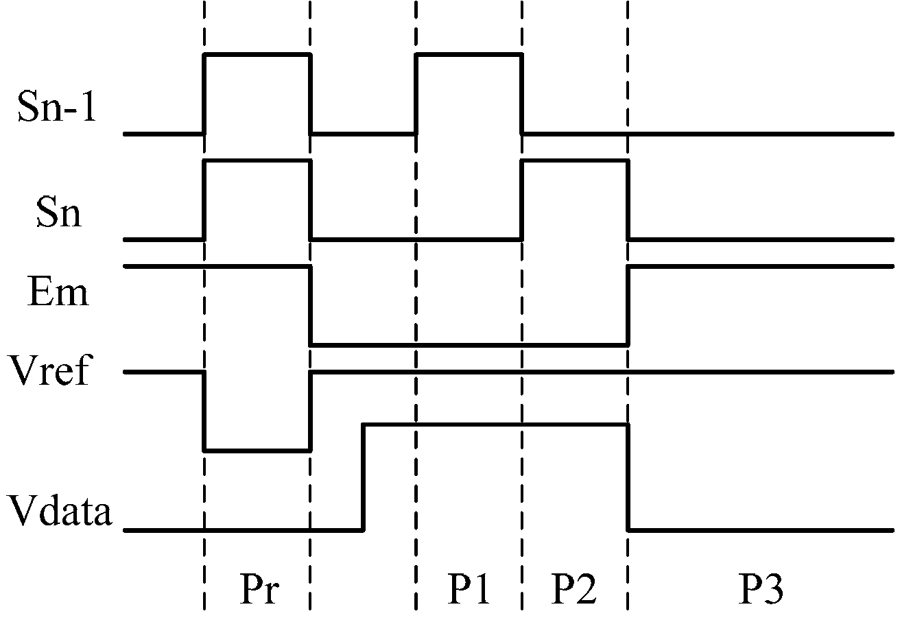
[0030] The following will clearly and completely describe the technical solutions in the embodiments of the present invention with reference to the accompanying drawings in the embodiments of the present invention. Obviously, the described embodiments are only some, not all, embodiments of the present invention. Based on the embodiments of the present invention, all other embodiments obtained by persons of ordinary skill in the art without making creative efforts belong to the protection scope of the present invention.

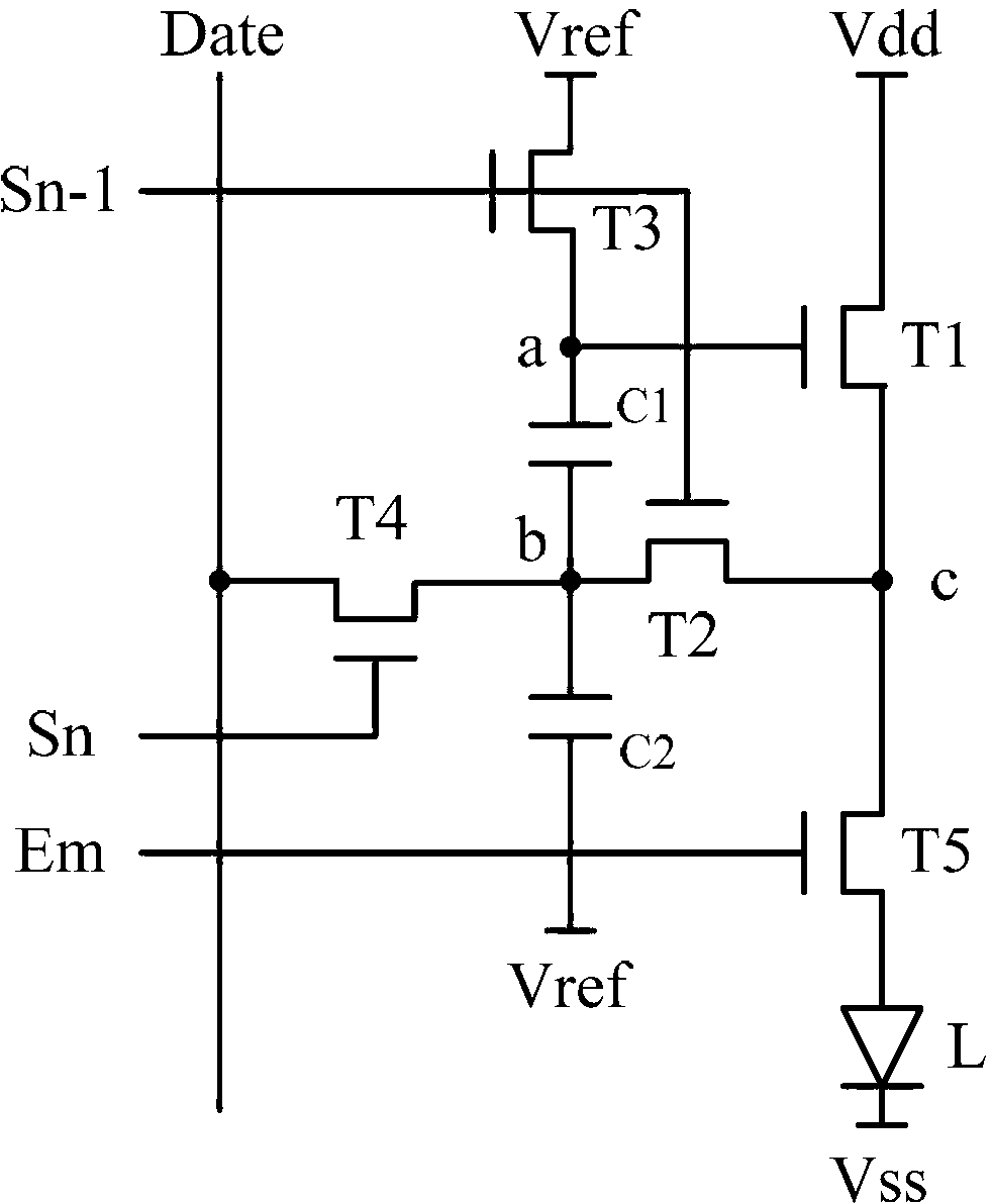
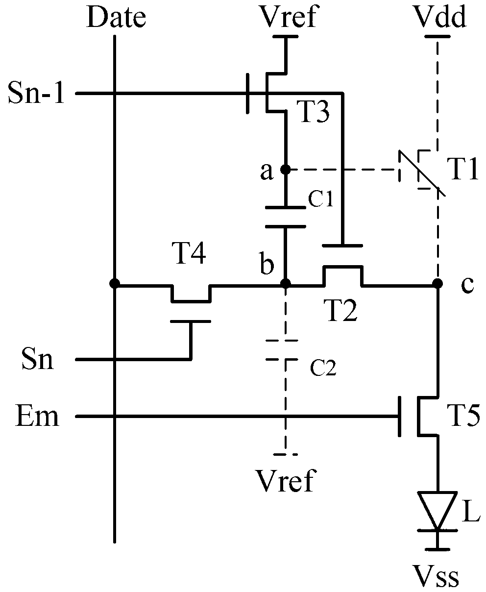
[0031] The pixel circuit 1 provided by the embodiment of the present invention, such as figure 1 shown, including:

[0032] The first transistor T1, the second transistor T2, the third transistor T3, the fourth transistor T4, the fifth transistor T5, the first storage capacitor C1, the second storage capacitor C2 and the light emitting device L.

[0033] The gate of the first transistor T1 is connected to the first pole of the third transistor T3, the first p...


PUM


Abstract

The invention discloses a pixel circuit, a driving method thereof and a display device, relates to the technical field of display, and aims to compensate for threshold voltage drift of a TFT (thin film transistor), improve uniformity of display lighting of the display device and prolong service life of the display device. The pixel circuit comprises a first transistor, a second transistor, a third transistor, a fourth transistor, a fifth transistor, a first storage capacitor, a second storage capacitor and a light emitting device. The pixel circuit, the driving method thereof and the display device are applied to manufacturing of display panels.

Description

technical field [0001] The present invention relates to the field of display technology, in particular to a pixel circuit, a driving method thereof, and a display device. Background technique [0002] With the rapid progress of display technology, semiconductor element technology, which is the core of the display device, has also been greatly improved. For existing display devices, Organic Light Emitting Diode (OLED) is a current-type light-emitting device, because of its self-illumination, fast response, wide viewing angle and the ability to be fabricated on flexible substrates, etc. characteristics and are increasingly being used in the field of high-performance displays. OLED can be divided into PMOLED (Passive Matrix Driving OLED, passive matrix driving organic light emitting diode) and AMOLED (Active Matrix Driving OLED, active matrix driving organic light emitting diode) according to the driving method. Due to the advantages of response speed, power saving, DC drive ...

Claims


Application Information

Patent Timeline
Patent Type & Authority Applications(China)
IPC IPC(8): G09G3/32
CPCG09G3/325G09G2310/0251G09G2310/0262G09G2310/067G09G2320/045H10K59/1216
Inventor 尹静文吴仲远段立业
Owner BOE TECH GRP CO LTD
Why Eureka
Try Eureka