
Array substrate, driving method thereof and display device
An array substrate and matrix technology, applied in the display field, can solve problems such as large voltage swing, and achieve the effect of reducing voltage swing and power consumption
Patent Information
- Authority / Receiving Office
- CN · China
- Patent Type
- Applications(China)
- Current Assignee / Owner
- Publication Date
- 2013-12-25
- Estimated Expiration
- Not applicable · inactive patent
Smart Images
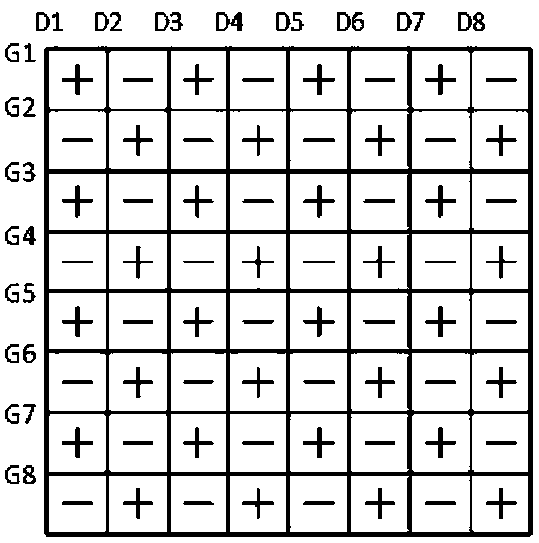
Figure 1 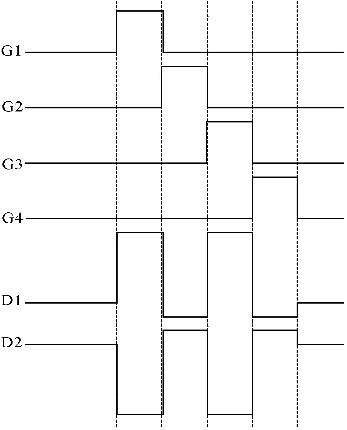
Figure 2 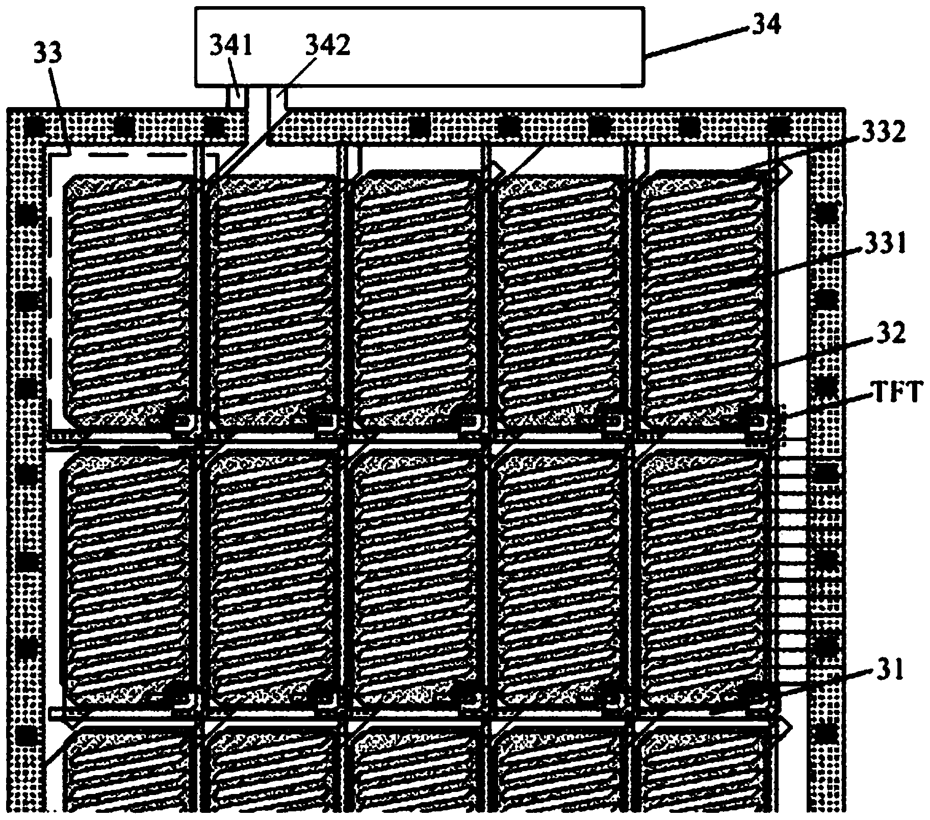
Figure 3
Abstract
Description
technical field
[0001] The present invention relates to the field of display technology, in particular to an array substrate, a driving method thereof, and a display device. Background technique
[0002] Liquid Crystal Display (LCD for short) is favored by engineers because of its low power consumption, light and thin appearance, and no radiation. Therefore, it has been widely used in various electronic products including computers, mobile phones, etc. in electronic equipment. Liquid crystal displays usually include an array substrate, a color filter substrate, and a liquid crystal layer located between the array substrate and the color filter substrate. The display principle is mainly to change the liquid crystal molecules in the liquid crystal layer by changing the potential difference between the two ends of the liquid crystal layer. The rotation angle of the liquid crystal changes the light transmittance of the liquid crystal to display different images.
[0003] Gener...
Examples
Embodiment Construction
[0023] The following will clearly and completely describe the technical solutions in the embodiments of the present invention with reference to the accompanying drawings in the embodiments of the present invention. Obviously, the described embodiments are only some, not all, embodiments of the present invention. All other embodiments obtained by persons of ordinary skill in the art based on the embodiments of the present invention belong to the protection scope of the present invention.
[0024] The array substrate provided by the embodiment of the present invention, such as image 3 As shown, it includes a plurality of pixel units 33 arranged in a matrix which are divided by a plurality of cross gate lines 31 and data lines 32, and each pixel unit 33 further includes a pixel electrode 331, wherein each pixel unit 33 A common electrode 332 is also included.
[0025] In the matrix of pixel units 33 , the voltage polarities of the common electrodes 332 corresponding to the pixe...