
Array substrate, display device and drive method of display device

A technology of array substrates and column data lines, applied in static indicators, nonlinear optics, instruments, etc., can solve the problem of small viewing angle of ADS-type liquid crystal display, and achieve the effect of increasing the viewing angle width

Inactive Publication Date: 2014-02-05
BOE TECH GRP CO LTD
View PDF5 Cites 4 Cited by
  • Summary
  • Abstract
  • Description
  • Claims
  • Application Information

AI Technical Summary

Problems solved by technology

[0005] The embodiment of the present invention provides an array substrate, a display device provided with the array substrate and a driving method thereof, which solves the technical problem of the existing ADS-type liquid crystal display with a small viewing angle

Method used


Image

  • Array substrate, display device and drive method of display device
  • Array substrate, display device and drive method of display device
  • Array substrate, display device and drive method of display device

Examples


Embodiment Construction

[0028] The technical solutions in the embodiments of the present invention will be clearly and completely described below in conjunction with the drawings in the embodiments of the present invention.

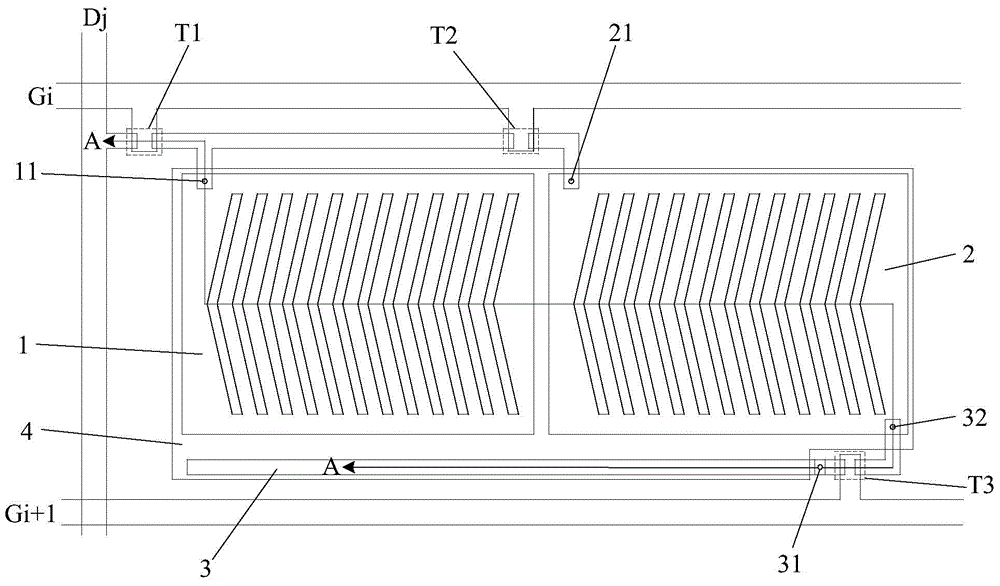
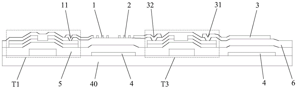
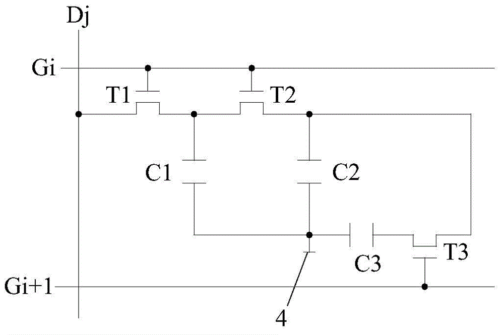
[0029] The array substrate provided by the embodiment of the present invention includes n+1 rows of gate lines and m columns of data lines, and n×m pixels arranged in an array. like figure 1 and figure 2 As shown, each pixel includes a first thin film transistor T1, a second thin film transistor T2, a third thin film transistor T3, a common electrode 4, and a first pixel electrode 1, a second pixel electrode 2 and a storage device corresponding to the common electrode 4. Electrode 3. In this embodiment, the first pixel electrode 1 , the second pixel electrode 2 and the storage electrode 3 are located above the common electrode 4 . The common electrode 4 is formed on the substrate (glass) substrate 40, the common electrode 4 is covered with a gate insulating layer 5 and a pas...


PUM


Abstract

An embodiment of the invention discloses an array substrate, a display device provided with the array substrate and a drive method of the display device, belongs to the technical field of display, and solves the technical problem of small view angles of existing ADS (advanced super dimension switch) liquid crystal displays. The array substrate comprises n+1 lines of grid lines, m rows of data lines as well as n*m pixels arranged in an array manner, wherein each pixel comprises a first thin film transistor T1, a second thin film transistor T2, a third thin film transistor T3, a common electrode, a first pixel electrode, a second pixel electrode and a storage electrode; in each pixel in the i line, grids of the T1 and the T2 are connected with the grid line in the i line, and the grid of the T3 is connected with the grid line in the (i+1) line; and in each pixel in the j row, the first and second pixel electrodes are connected with the data line in the j row respectively through the T1 and the T2, and the second pixel electrode is connected with the storage electrode through the T3. The array substrate can be applied to the display devices such as liquid crystal display televisions, liquid crystal displays, digital photo frames, mobile phones, tablet personal computers and the like.

Description

technical field [0001] The invention belongs to the field of display technology, and in particular relates to an array substrate, a display device provided with the array substrate and a driving method thereof. Background technique [0002] With the continuous development of display technology, thin film transistor liquid crystal display (Thin Film Transistor Liquid Crystal Display, TFT-LCD) has the advantages of small size, low power consumption, no radiation, etc., and occupies a dominant position in the field of flat panel display. Among them, the advanced super dimension switch (Advanced super Dimension Switch, ADS) type liquid crystal display has the advantages of wide viewing angle, high aperture ratio, high transmittance, etc., and is widely used. [0003] Currently, in pixels of an ADS-type liquid crystal display, liquid crystal molecules are usually designed in a single-domain or two-domain manner. In the driving process of the ADS liquid crystal display, a certain...

Claims


Application Information

Patent Timeline
Patent Type & Authority Applications(China)
IPC IPC(8): G02F1/1362G02F1/1343G02F1/133
Inventor 程鸿飞
Owner BOE TECH GRP CO LTD
Features
  • Generate Ideas
  • Intellectual Property
  • Life Sciences
  • Materials
  • Tech Scout
  • Unparalleled Data Quality
  • Higher Quality Content
  • 60% Fewer Hallucinations
Learn More