Pre-injection molding type MINI LED packaging substrate
A packaging substrate and pre-injection technology, applied in electrical components, electrical solid devices, circuits, etc., can solve the problems of low reliability, large pixel pitch, low resolution, etc. The effect of a wide viewing angle range
- Summary
- Abstract
- Description
- Claims
- Application Information
AI Technical Summary
Problems solved by technology
Method used
Image

Examples
Embodiment Construction
[0044] Next, the technical solutions in the embodiments in the embodiments will be described in contemplation in conjunction with the drawings of the present invention.
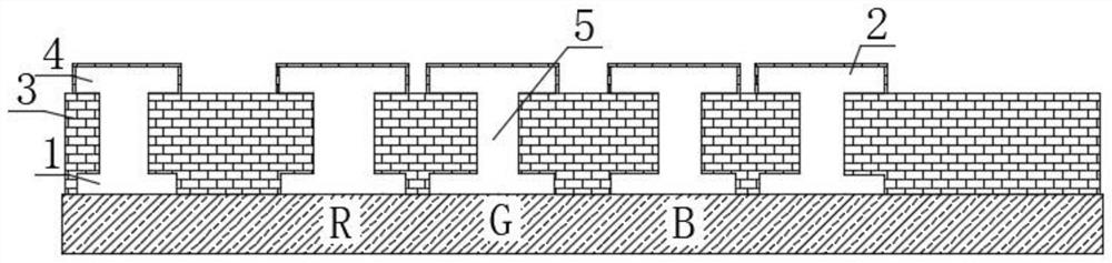
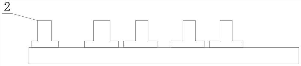
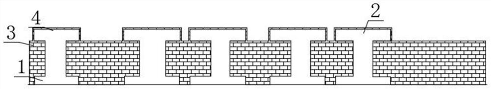
[0045] See Figure 1 ~ 5 In the present invention, the pre-plastic MINI LED package substrate includes pad 1 and package line structure 2, and the pad 1 is formed by etching, and the gap of the package line structure 2 is filled with a polymer layer 3. The package line structure 2 is integrated with a plurality of pins 4, and the pad 1 is provided with a thermal post 5, and the spacing of adjacent pin 4 is less than 0.3 mm, and the package line structure 2 and the polymer layer 3 are coarse Treatment.
[0046] The flat packaging scheme is used to remove the traditional groove package design, which greatly widened the range of view, and the surface-roughened treatment process, the interface binding force of different materials is used by the specific surface area of the roughness. Increased, enhanced binding powe...
PUM
 Abstract
Description
Claims
Application Information