Wiring system and method based on ink-jet printing and selective laser melting

A technology of laser melting and inkjet printing, applied in printing, typewriters, etc., can solve problems such as cumbersome procedures, achieve efficient wiring methods, high-precision wiring methods, and reduce the effect of impact

Active Publication Date: 2014-12-24
CHONGQING INST OF GREEN & INTELLIGENT TECH CHINESE ACADEMY OF SCI
View PDF6 Cites 9 Cited by
  • Summary
  • Abstract
  • Description
  • Claims
  • Application Information

AI Technical Summary

Problems solved by technology

However, this method still needs to go through two processes of inkjet wiring and selective heat treatment, and the selective heat treatment process needs to reposition the scanning path, which is relatively cumbersome in program

Method used


Image

  • Wiring system and method based on ink-jet printing and selective laser melting
  • Wiring system and method based on ink-jet printing and selective laser melting

Examples


example 1

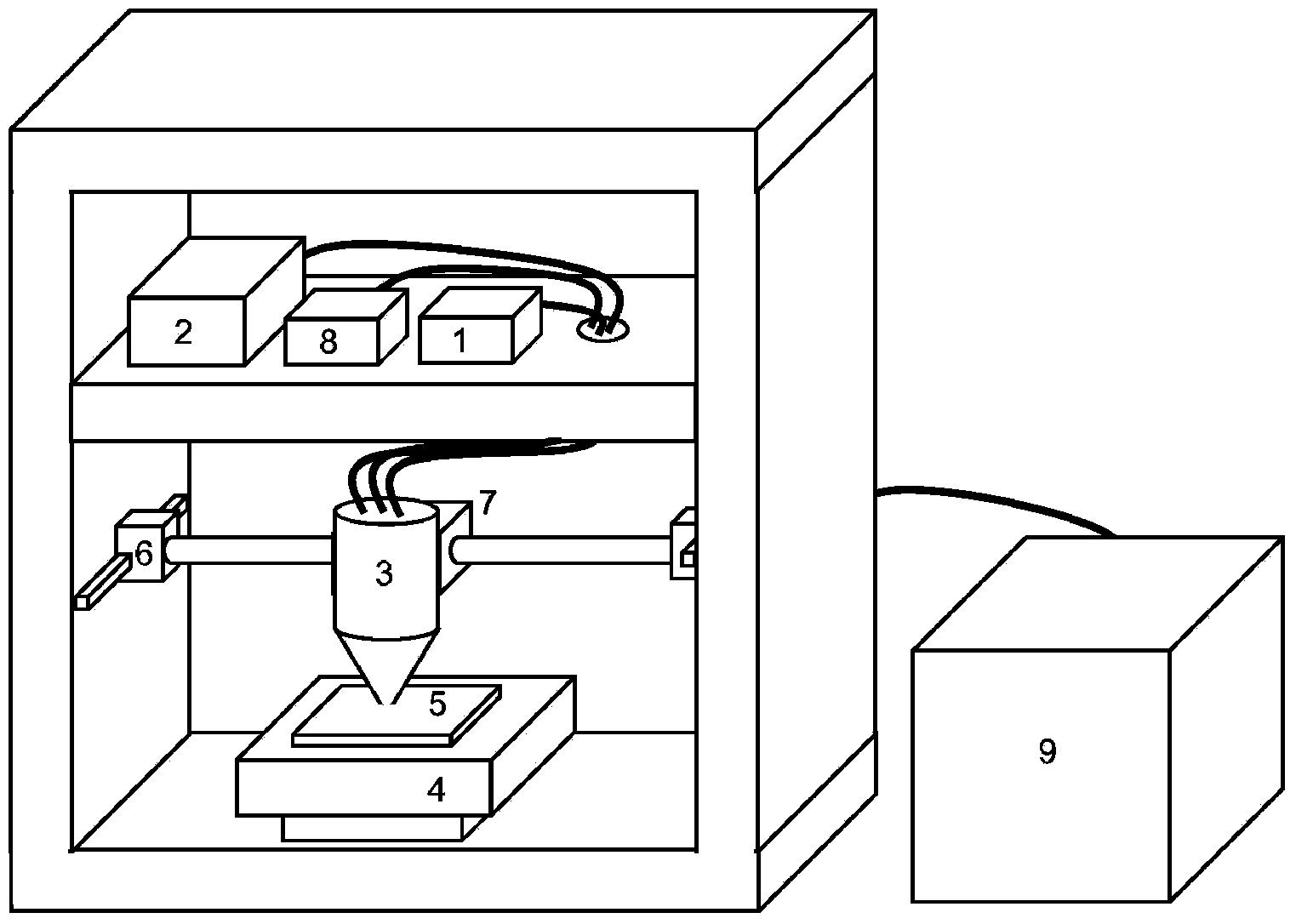
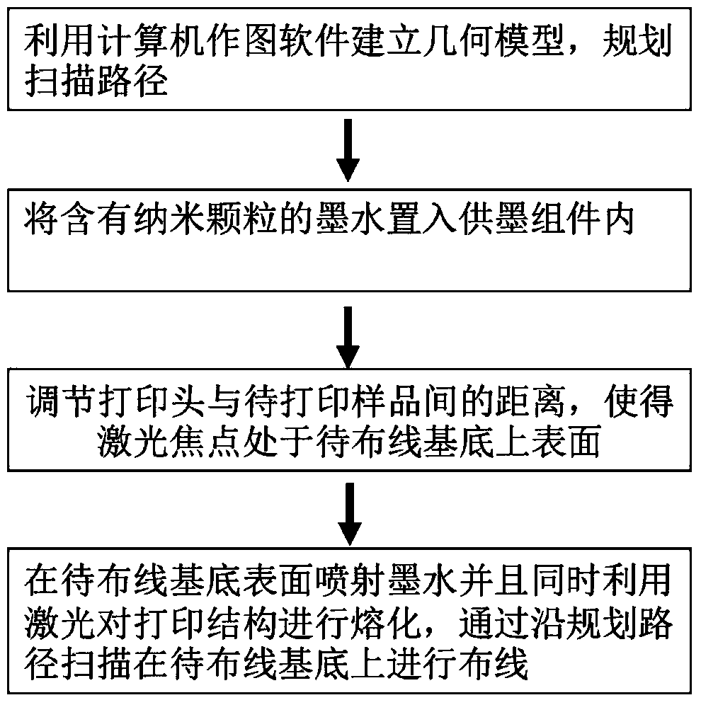
[0052] Combine the following figure 1 and figure 2 , the present invention will be described in detail by taking the silver metal wiring on the glass substrate by using the wiring method based on inkjet printing and selective laser melting as an example.

[0053] First, use computer graphics software to establish a geometric model and plan the scanning path;

[0054] Ink containing silver nanoparticles with a particle size of 1 to 10 nm is placed in the ink supply assembly 1;

[0055] Move the lifting angle displacement table 4 through computer control, adjust the distance between the printing head 3 and the glass substrate 5 to be 0.1mm to 1mm, so that the laser focus is on the upper surface of the glass substrate;

[0056] Ink is sprayed on the upper surface of the glass substrate 5 to be prepared and at the same time, the structure is irradiated and melted with an 808nm focused laser with a power of 20W to 60W, and the laser focal spot size is 0.1mm to 1mm;

[0057] The...

Embodiment 2

[0059] refer to figure 1 and figure 2 , the present invention will be described in detail by taking copper metal wiring on a hemispherical crown-shaped plastic substrate by using a wiring method based on inkjet printing and selective laser melting as an example.

[0060] First, use computer graphics software to establish a geometric model and plan the scanning path;

[0061] Put the ink containing copper nanoparticles with a particle size of 1 to 10 nm into the ink supply assembly 1;

[0062] Controlled by a computer to move the lifting angle displacement table 4, adjust the distance between the print head 3 and the highest point 5 of the hemispherical crown-shaped plastic base to be 0.1mm-1mm, so that the laser focus is on the upper surface of the highest point of the hemispherical crown-shaped plastic base;

[0063] Spray ink on the upper surface of the hemispherical crown-shaped plastic substrate 5 and at the same time use an 808nm focused laser with a power of 20W to 60...


PUM


Abstract

The invention provides a wiring system and method based on ink-jet printing and selective laser melting. The system comprises an ink supply component, a laser source, a printing head, a monitoring component, a lifting angle displacement table, a suspension component, a printing head moving component and a computer. The method comprises the following steps that computer plotting software is used for establishing a geometric model, and a scanning route is planned; ink with nano-particles is placed into the ink supply component; the distance between the printing head and a substrate where wiring is to be carried out is adjusted, so that a laser focus is placed on the upper surface of the substrate where wiring is to be carried out; and ink is sprayed to the surface of the substrate where wiring is to be carried out, meanwhile, laser is used for melting a printing structure, and by scanning along the planned route, wiring is carried out on the substrate where wiring is to be carried out. Ink-jet printing and selective laser melting are combined, structure ink-jet printing and melting heat processing can be achieved at the same time, the wiring method is simple, efficient and high in accuracy, and influence on the substrate from a processing course is lowered by selective heat processing of laser.

Description

technical field [0001] The invention relates to a direct wiring system and method, in particular to a wiring system and method based on inkjet printing and selective laser melting. Background technique [0002] Selective wiring directly on the structure is of great significance to realize the functionalization and function expansion of the structure. Selective routing has important applications in electronics, optical devices, metamaterials, plasmon photonics, etc. [0003] Inkjet printing technology is an important selective wiring method. It prints the ink containing metal nanoparticles onto the surface of the carrier structure by controlling the scanning of the printing head or the nozzle. High, and due to the existence of the interface between particles, its electrical conductivity and other properties are also greatly affected. At present, in order to improve the performance of inkjet printed structures, it is generally achieved through subsequent heat treatment. Sub...

Claims


Application Information

Patent Timeline
Patent Type & Authority Applications(China)
IPC IPC(8): B41J2/01B41J2/435B41J3/00
Inventor 段宣明曹洪忠曹良成徐佼刘基权
Owner CHONGQING INST OF GREEN & INTELLIGENT TECH CHINESE ACADEMY OF SCI
Why Eureka
Try Eureka