Apparatus and method for processing wafer

A technology of wafer processing and processing methods, which is applied in the direction of electrical components, semiconductor/solid-state device manufacturing, circuits, etc., can solve the problem of increasing the area of ​​the device, and achieve the effect of saving space and high-efficiency irradiation

Active Publication Date: 2015-09-16
DISCO CORP
View PDF8 Cites 5 Cited by
  • Summary
  • Abstract
  • Description
  • Claims
  • Application Information

AI Technical Summary

Problems solved by technology

[0004] However, the cutting device described in Patent Document 1 requires installation space so that the ultraviolet irradiation unit can be incorporated, and there is a problem that the area of ​​the device increases as the wafer diameter increases.

Method used


Image

  • Apparatus and method for processing wafer
  • Apparatus and method for processing wafer
  • Apparatus and method for processing wafer

Examples


Embodiment Construction

[0017] Hereinafter, modes (embodiments) for carrying out the present invention will be described in detail with reference to the drawings. The present invention is not limited to the contents described in the following embodiments. In addition, the structural elements described below include elements that are easily conceived by those skilled in the art and actually the same elements. Furthermore, the configurations described below may be appropriately combined. In addition, various omissions, substitutions, or changes in the structure can be made without departing from the gist of the present invention.

[0018] [implementation mode]

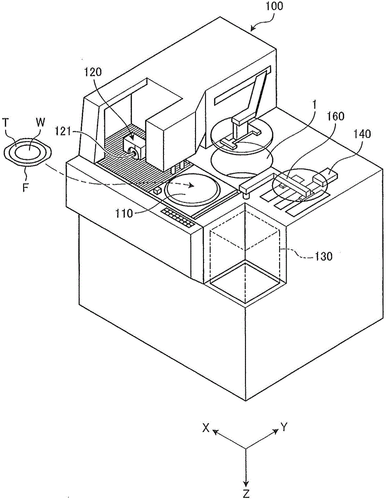
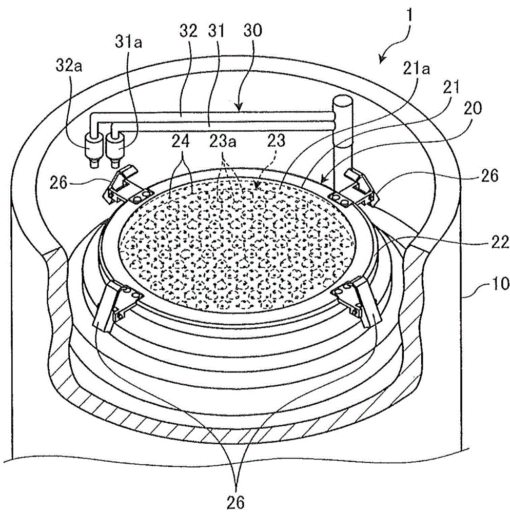
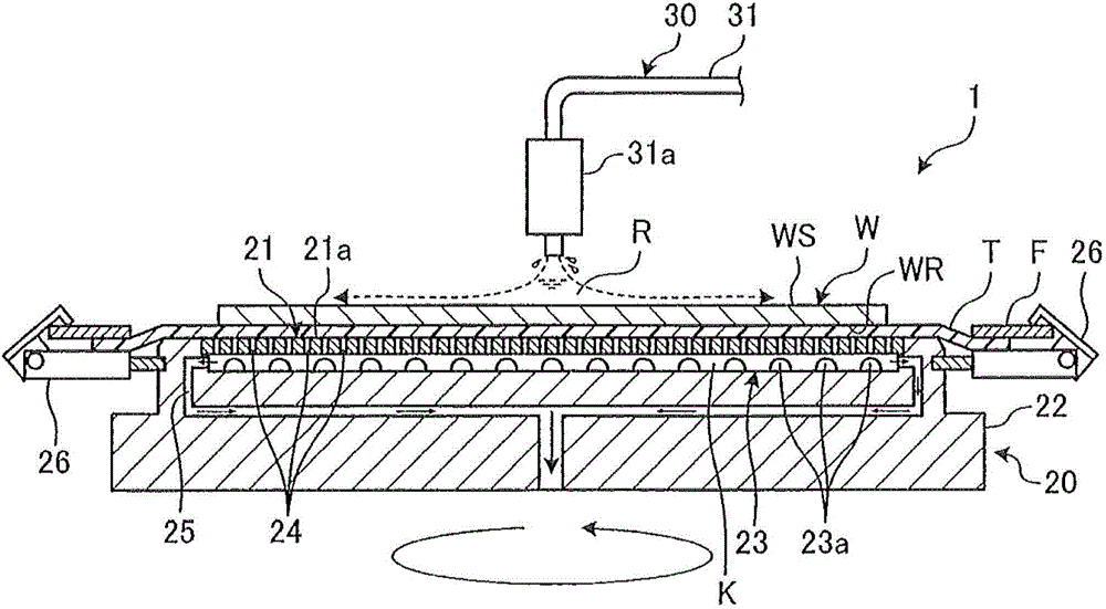
[0019] A wafer processing apparatus and a wafer processing method according to an embodiment of the present invention will be described with reference to the drawings. figure 1 It is a perspective view of a configuration example of a cutting device provided with a cleaning device as a wafer processing device according to the embodiment. fi...


PUM


Abstract

The invention provides an apparatus and method for processing a wafer, which can efficiently irradiate ultraviolet light under the condition of not enlarging an apparatus area. A cleaning apparatus (1) of a wafer apparatus is provided with a cleaning unit; the cleaning unit cleans and dries the holding bench (20) of a held wafer (W) and a front side (WS) of the held wafer (W) on the holding bench (20). The holding bench (20) is provided with a holding part (21) and an ultraviolet light irradiation part (23). The holding part (21) is provided with a holding surface (21a) and is formed through materials capable of penetrating ultraviolet light (U), wherein the holding surface (21a) is provided with a plurality of suction holes (24) used for absorbing and holding the back surface (WR) of the wafer (W) to keep a whole back surface (WR). The ultraviolet light irradiation part (23) is configured on an opposite side of the holding surface (21a) of the holding part (21).

Description

technical field [0001] The present invention relates to a wafer processing apparatus for cleaning the front surface of a wafer and a wafer processing method. Background technique [0002] In the chipping device, after chipping the wafer held on the frame, ultraviolet rays are irradiated to the tape to which the chip is attached to reduce its viscosity, thereby facilitating the chip pickup after chipping and improving workability. There has also been proposed a cutting device in which, in order to improve productivity, an ultraviolet irradiation unit is incorporated into the cutting device and an ultraviolet irradiation area is provided, and a wafer that has been cut can be irradiated with ultraviolet light (for example, by using the standby time during wafer cutting). , refer to Patent Document 1). [0003] Patent Document 1 Japanese Patent Application Laid-Open No. 07-45556 [0004] However, the cutting device described in Patent Document 1 requires installation space to ...

Claims


Application Information

Patent Timeline
Patent Type & Authority Applications(China)
IPC IPC(8): H01L21/67H01L21/02
CPCH01L21/67H01L21/67034H01L21/68757H01L21/68785H01L21/67057H01L21/6836H01L21/6838
Inventor 铃木稔
Owner DISCO CORP
Why Eureka
Try Eureka