
Negative Voltage Clamp Circuit

A clamp circuit and negative voltage technology, applied in the field of new negative voltage clamp circuit, can solve the problems of abnormal chip operation and unstable lithium battery protection system.

Active Publication Date: 2017-12-12
SINO WEALTH ELECTRONICS
View PDF6 Cites 0 Cited by
  • Summary
  • Abstract
  • Description
  • Claims
  • Application Information

AI Technical Summary

Problems solved by technology

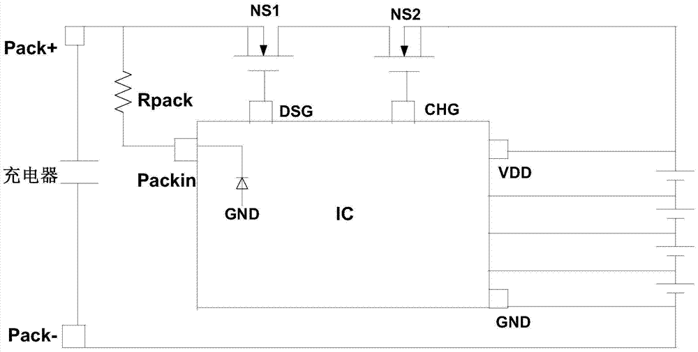
[0004] The negative voltage of the positive terminal PACK+ of the battery pack is transmitted to the chip port Packin through the resistance Rpack, and the internal ESD circuit of the chip port Packin forms a diode conduction from the P substrate to the chip port Packin, which generates a substrate current and causes the internal operation of the chip (IC) to be abnormal. Causes the entire lithium battery protection system to be unstable

Method used


Image

  • Negative Voltage Clamp Circuit
  • Negative Voltage Clamp Circuit

Examples


Embodiment Construction

[0026] The present invention will be further described below in conjunction with specific embodiment and accompanying drawing, set forth more details in the following description so as to fully understand the present invention, but the present invention can obviously be implemented in many other ways different from this description, Those skilled in the art can make similar promotions and deductions based on actual application situations without violating the connotation of the present invention, so the content of this specific embodiment should not limit the protection scope of the present invention.

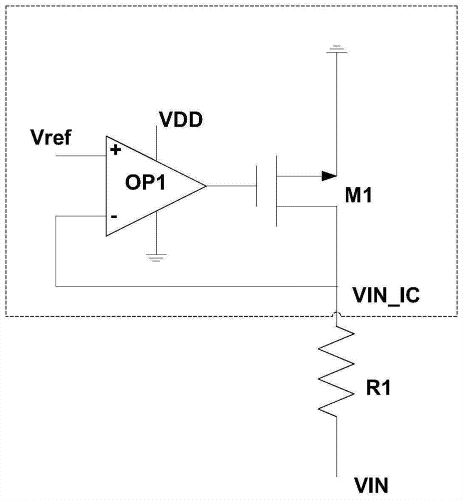
[0027] figure 2 It is a schematic structural diagram of a negative voltage clamping circuit according to an embodiment of the present invention. Such as figure 2 As shown, the negative voltage clamping circuit 200 mainly includes an NMOS transistor M1, an external current limiting resistor R1 and an operational amplifier OP1. Wherein, the positive input terminal of the oper...


PUM


Abstract

The invention provides a negative voltage clamping circuit comprising an NMOS tube, an external current-limiting resistor and an operational amplifier. The positive input terminal of the operational amplifier is connected to a voltage reference, the negative input terminal of the operational amplifier is connected to a chip port, and the output terminal of the operational amplifier is connected to the grid electrode of the NMOS tube. The source electrode of the NMOS tube is grounded, and the drain electrode of the NMOS tube is connected to the chip port. The chip port is outwardly connected to the external current-limiting resistor, and the external current-limiting resistor is connected to an external input voltage. According to the invention, the external negative voltage is clamped through the negative feedback technology, and a chip cannot be influenced by the negative voltage.

Description

technical field [0001] The invention relates to the technical field of analog integrated circuits, in particular, the invention relates to a novel negative voltage clamping circuit. Background technique [0002] All circuits in an integrated circuit are made on the same substrate, usually a P-type substrate. In order to isolate the internal circuit and ensure the reverse bias of the PN junction, the P-type substrate is generally grounded. In order to prevent the IC port from being damaged due to static electricity accumulation, an ESD circuit needs to be added to the IC port. Use the forward conduction and reverse breakdown characteristics of the diode to discharge the forward and negative voltage spikes of the IC port. If a negative voltage is applied to the IC port, the diode to ground will be turned on, and current will flow through the P-type substrate. All internal circuits are made on a P-type substrate, and this current will affect its work, especially high-precisi...

Claims


Application Information

Patent Timeline
Patent Type & Authority Patents(China)
IPC IPC(8): G05F1/56
Inventor 罗彦
Owner SINO WEALTH ELECTRONICS
Learn More