
Control method of thin-layer epitaxial transition region on heavily doped phosphorous substrate
A transition zone and substrate technology, applied in electrical components, semiconductor/solid-state device manufacturing, circuits, etc., can solve the problems of limited transition zone steepness, increased TCS flow, TCS waste, etc., to improve BVDS discreteness, increase Edge resistivity value, the effect of reducing the effect of self-doping
- Summary
- Abstract
- Description
- Claims
- Application Information
AI Technical Summary
Problems solved by technology
Method used
Image

Examples
Embodiment 1
[0029] The invention discloses a control method of a thin-layer epitaxial transition region of a heavily doped phosphorus substrate, which comprises the following steps:
[0030] 1) The temperature and TCS (trichlorosilane) flow rate of the monolithic epitaxial growth system are fixed when the substrate is epitaxially grown.
[0031] 2) During epitaxial growth of the substrate, the same doping process is used for the growth of the cover layer and the growth of the epitaxial layer.
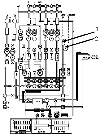
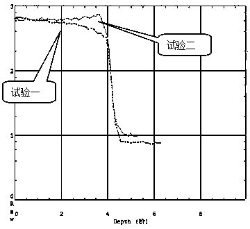
[0032] 3) During the growth of the epitaxial layer, change the bypass discharge (exhaust) pressure in the monolithic epitaxial growth system, so that the bypass discharge pressure is greater than or less than the system cavity (cavity) pressure, and adjust the steepness of the transition zone of the epitaxial layer degree.
[0033] 4) By adjusting the bypass discharge pressure, changing the steepness of the transition region of the epitaxial layer, and analyzing the extended resistance profile of ...
Embodiment 2
[0035] The invention discloses a control method of a thin-layer epitaxial transition region of a heavily doped phosphorus substrate, which comprises the following steps:
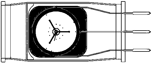
[0036] Using ASM E2000 type monolithic epitaxial growth system, such as figure 1 As shown, the infrared lamp array is radiatively heated, the high-purity graphite base is a silicon wafer carrier, and the protective gas is ultra-high-purity H 2 , the purity reaches more than 99.999999%.
[0037] Using 8-inch heavily doped phosphorus substrate, crystal orientation , resistivity range of 0.001-0.0015ohm.cm, super hermetic back-sealing process;
[0038] Before epitaxial growth, the system is fully removed from the doping treatment. At 1190 ° C, a large flow of HCL gas is introduced at 20 slm / min, and when the residual Si and the residual Si on the base are etched away, the H 2 The flow rate is set to 10slm / min, and when corroding the residual Si on the inner wall of the bell jar, increase the H 2 The flow rat...
PUM
 Abstract
Description
Claims
Application Information