Shifting register and grid driving circuit

A gate drive circuit, shift register technology, applied in static memory, digital memory information, instruments, etc., can solve problems such as affecting display quality, writing wrong grayscale values ​​in falling time pixels, etc.

CN106782280AActive Publication Date: 2017-05-31AU OPTRONICS CORP
14 Cites 17 Cited by

Patent Information

Authority / Receiving Office
CN · China
Patent Type
Applications(China)
Current Assignee / Owner
Publication Date
2017-05-31

Smart Images

  • Figure 1
    Figure 1
  • Figure 2
    Figure 2
  • Figure 3
    Figure 3
Patent Text Reader

Abstract

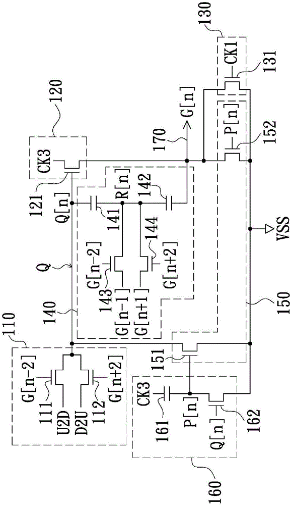
The invention provides a shifting register and grid driving circuit adopting the same. The shifting register comprises an input signal selection circuit, an output circuit, a pull-down circuit and a voltage raising circuit. The input signal selection circuit is coupled to a node, a first signal source, a second signal source, a first input signal source and a second input signal source. The output circuit is coupled to the node, the output end of the shifting register and the first clock source. The pull-down circuit is coupled to the output end, the second clock source and a reference potential source. The voltage raising circuit is coupled to the node, the output end, the first signal source, the second signal source, the third signal source and the fourth signal source. The shifting register provided by the present invention can shorten the falling time of the pulses it provides.
Need to check novelty before this filing date? Find Prior Art

Description

technical field

[0001] The present invention relates to related technologies of displays, in particular to a shift register and a gate drive circuit using the shift register. Background technique

[0002] The gate drive circuit used in the display is composed of a plurality of shift registers, each shift register is used to output a gate signal, and a pulse is provided through the gate signal to turn on the pixels of the corresponding column to Each pixel in the row of pixels can write the required gray scale value.

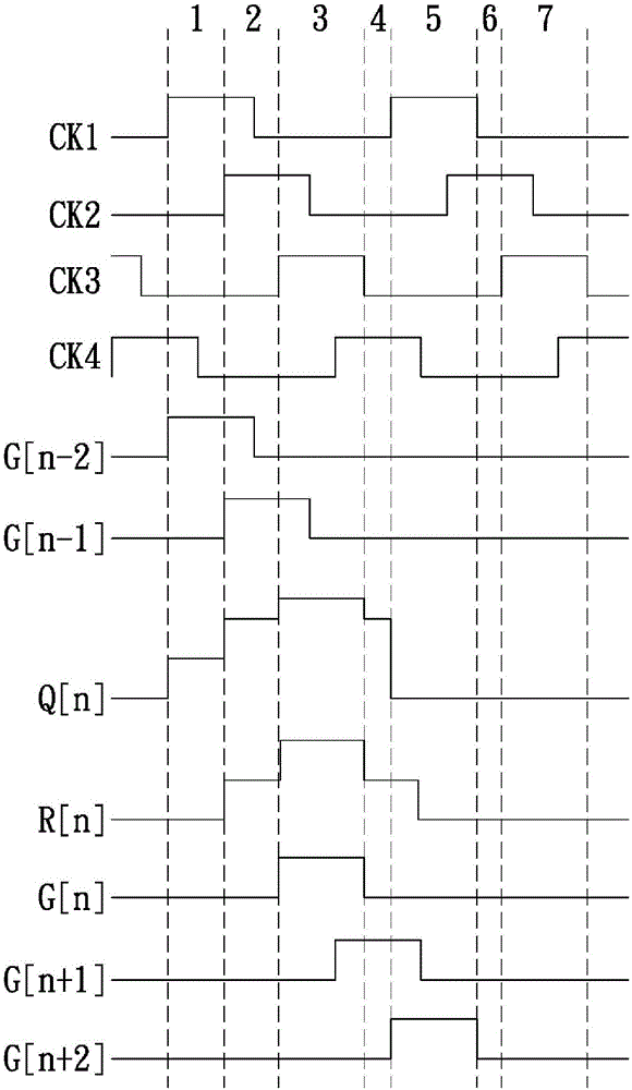
[0003] However, under the traditional shift register circuit structure, when the shift register turns the pulse provided by it from high level to low level, the falling time of the bit pulse is too long and the pixel Wrong grayscale values ​​are written, thereby affecting the display quality, and this shortcoming is especially obvious in high-resolution displays. Contents of the invention

[0004] An object of the present invention is to provide a shift reg...

Examples

Embodiment Construction

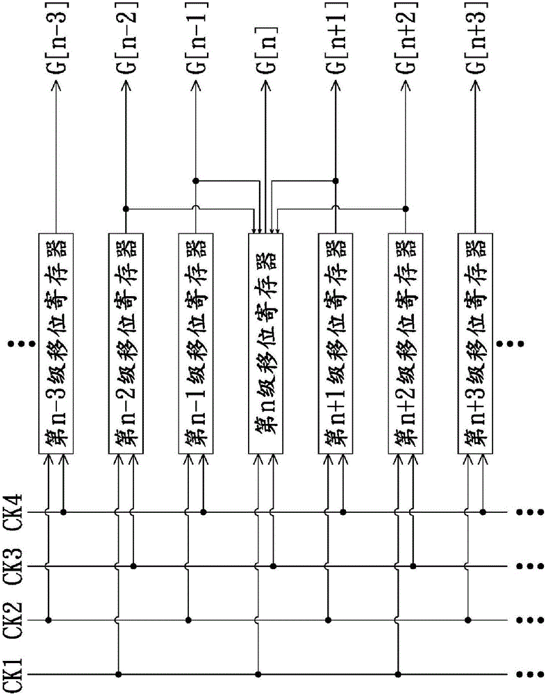
[0030] To make it easy for readers to understand, the gate driving circuit of the present invention will be described first. figure 1 It is a circuit diagram of a shift register according to an embodiment of the present invention, such as figure 1 As shown, the gate drive circuit is composed of multiple shift registers. figure 1 Only the n-3th stage shift register to the n+3th stage shift register is shown in , and only the complete coupling mode of the nth stage shift register is shown, while the complete coupling of the remaining shift registers The connection method can be simulated and deduced according to the following description, and will not be repeated here.

[0031] Such as figure 1 As shown, the n-2th shift register, the n-th shift register and the n+2-th shift register all receive the clock signals CK1 and CK3, while the n-3th shift register, the n-th The first-stage shift register, the n+1-th stage shift register and the n+3-th stage shift register all receive ...