Liquid crystal display panel and display device

A liquid crystal display panel, area technology, applied in instruments, nonlinear optics, optics, etc., can solve problems such as poor display of horizontal blocks and voltage differences, and achieve the effect of offsetting resistance differences and solving voltage differences.

Active Publication Date: 2020-05-22
TCL CHINA STAR OPTOELECTRONICS TECH CO LTD
View PDF3 Cites 0 Cited by
  • Summary
  • Abstract
  • Description
  • Claims
  • Application Information

AI Technical Summary

Problems solved by technology

[0006] The present invention provides a liquid crystal display panel. By changing the area covered by the edge area of ​​the common electrode on the array substrate, the capacitance value of the substrate wiring and the fan-out wiring is adjusted to offset the difference in resistance value and solve the problem of input voltage caused by the difference in resistance value. There is a difference in the voltage to the inside of the panel, which leads to poor display of horizontal blocks

Method used


Image

  • Liquid crystal display panel and display device
  • Liquid crystal display panel and display device
  • Liquid crystal display panel and display device

Examples


Embodiment Construction

[0046] The following descriptions of the various embodiments refer to the accompanying drawings to illustrate specific embodiments in which the invention may be practiced. The directional terms mentioned in the present invention, such as [top], [bottom], [front], [back], [left], [right], [inside], [outside], [side], etc., are only for reference The orientation of the attached schema. Therefore, the directional terms used are used to illustrate and understand the present invention, but not to limit the present invention. In the figures, structurally similar elements are denoted by the same reference numerals.

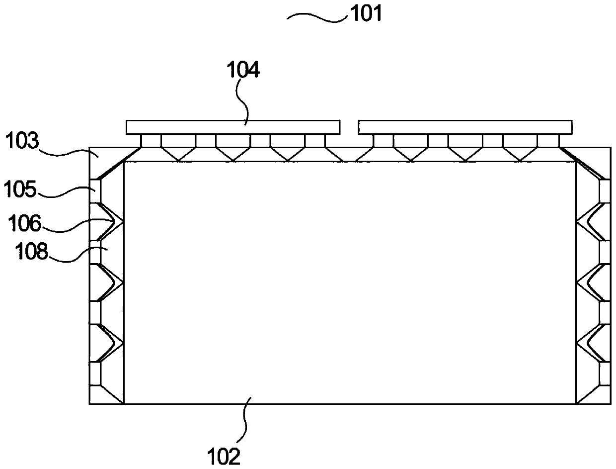
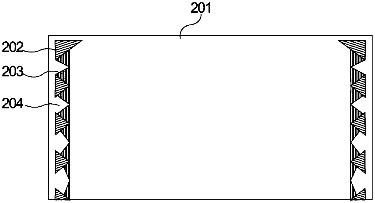
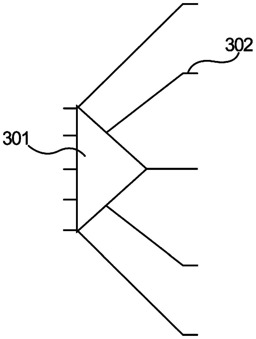
[0047] The present invention is aimed at the existing liquid crystal display panel. Due to the difference in resistance between the substrate wiring of the panel and the fan-out wiring, the signal delays at different positions of the panel are different, resulting in a difference in the voltage input to the inside of the panel, resulting in a horizontal block Bad pheno...


PUM


Abstract

The invention provides a liquid crystal display panel which comprises an array substrate and a color film substrate. The array substrate is provided with substrate routing and multiple gate pole chip on films, the surface of the color film substrate is provided with a common electrode layer which covers the substrate routing area and is of a hollowed-out structure, and then the area of the common electrode layer projected on the array substrate fringe area is reduced, so that a capacitance value between the common electrode layer and the substrate routing is adjusted. The liquid crystal display panel and the display device have the advantages that for the liquid crystal display panel, the capacitance value between the common electrode layer and the substrate routing is changed through the hollowed-out structure of the common electrode layer, a capacitance value difference is offset, and the technical problem that due to the fact that a difference caused by the capacitance value difference exists in voltage input into the panel, the display phenomenon of being poor in horizontal block is solved.

Description

technical field [0001] The invention relates to the field of liquid crystal display technology, in particular to a liquid crystal display panel and a display device with the liquid crystal display panel. Background technique [0002] With the development of display technology, liquid crystal displays have become the most common flat panel display devices. In a liquid crystal display, each pixel is controlled by grid lines and data lines criss-crossing on the substrate to realize image display. [0003] At present, in order to save costs, the gate drive circuit and the data circuit are often manufactured on the same printed circuit board, and then the circuit board is connected with the circuit board for transmitting the gate drive signal by using the wire on array (WOA for short). Gate Chip On Film (Gate Chip On Film, referred to as G-COF) connection. A liquid crystal display generally includes at least two COFs for transmitting gate driving signals, and two adjacent COFs ...

Claims


Application Information

Patent Timeline
Patent Type & Authority Patents(China)
IPC IPC(8): G02F1/1343G02F1/1345G02F1/1362
CPCG02F1/134309G02F1/13452G02F1/1362
Inventor 安立扬
Owner TCL CHINA STAR OPTOELECTRONICS TECH CO LTD
Why Eureka
Try Eureka