Pixel arrangement structure for OLED display panel, and OLED display panel

A pixel arrangement and display panel technology, which is applied in semiconductor devices, electrical components, circuits, etc., can solve the problems of increasing the difficulty and cost of the display panel process, achieve performance, high performance, and reduce process difficulty and cost.

A pixel arrangement and display panel technology, which is applied in semiconductor devices, electrical components, circuits, etc., can solve the problems of increasing the difficulty and cost of the display panel process, achieve performance, high performance, and reduce process difficulty and cost.

CN107293571AActive Publication Date: 2017-10-24TCL CHINA STAR OPTOELECTRONICS TECH CO LTD

Image

  • Pixel arrangement structure for OLED display panel, and OLED display panel
  • Pixel arrangement structure for OLED display panel, and OLED display panel
  • Pixel arrangement structure for OLED display panel, and OLED display panel

Examples


Embodiment Construction

[0024] The implementation of the present invention will be described in detail below in conjunction with the accompanying drawings and examples, so as to fully understand and implement the implementation process of how to apply technical means to solve technical problems and achieve corresponding technical effects in the present invention. The embodiments of the present application and the various features in the embodiments can be combined with each other under the premise of no conflict, and the formed technical solutions are all within the protection scope of the present invention.

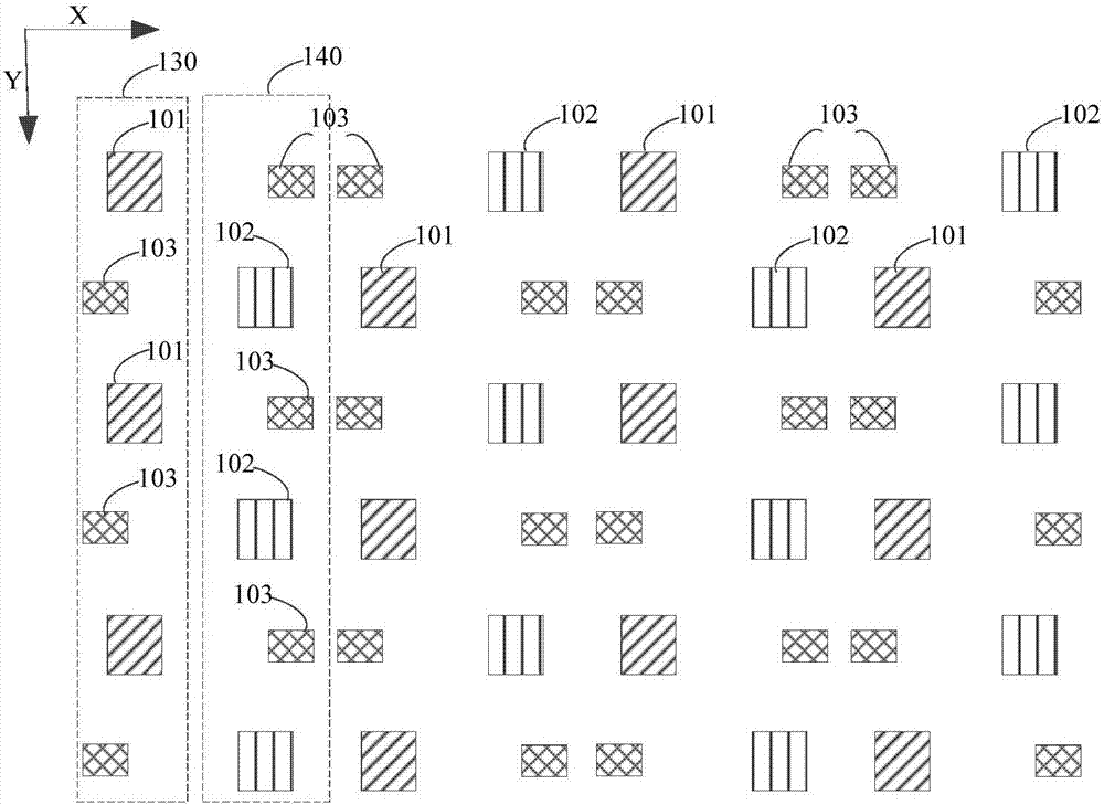
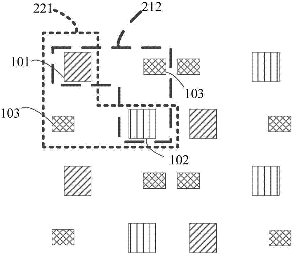
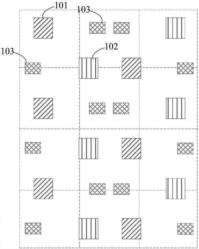
[0025] figure 1 It is a schematic diagram of a pixel arrangement structure of an OLED display panel according to an embodiment of the present invention.

[0026] like figure 1 As shown, each rectangle represents a sub-pixel. In this embodiment, a plurality of sub-pixels collectively form a sub-pixel array structure with multiple rows and multiple columns. The sub-pixels include a plurality o...


PUM


Abstract

The invention discloses a pixel arrangement structure for an OLED display panel, and the OLED display panel. The pixel arrangement structure comprises a plurality of first subpixels, a plurality of second subpixels, and a plurality of third subpixels. The first and second subpixels are alternately arranged in the row direction of the display panel, and a gap between the first and second subpixels which are selected at intervals is provided with two third subpixels in the row direction. The first and third subpixels are alternately arranged in the column direction of the display panel to form a first sequence, and the second and third subpixels are alternately arranged to form a second sequence. The first and second sequences are alternately arranged in the row direction. The structure provided by the invention can achieve the high-pixel-resolution presentation capability through a smaller number of subpixels, and reduces the technological difficulty and cost in preparation of a high-resolution display panel.

Description

technical field [0001] The invention belongs to the field of display technology, in particular to a pixel arrangement structure of an OLED display panel and the OLED display panel. Background technique [0002] With the continuous development of OLED display technology, the demand for resolution continues to increase. The resolution of an OLED display panel screen is usually expressed as the product of the number of pixels in the horizontal and vertical directions. In the traditional pixel design, a pixel unit is composed of three sub-pixels of R, G, and B. In this way, if the traditional arrangement of RGB pixels is adopted, in order to achieve high-resolution performance, the sub-pixel density of the display panel must be doubled, thereby significantly increasing the process difficulty and cost of manufacturing the display panel. Contents of the invention [0003] One of the technical problems to be solved by the present invention is to optimize the arrangement of sub-...

Claims


Application Information

Patent Timeline
24 Oct 2017
Publication
CN107293571A
IPC
H01L27/32
CPC
H10K59/353; H10K59/352
Inventors
金羽锋