AMOLED display device and driving method thereof

A technology of a display device and a driving method, which is applied to static indicators, instruments, semiconductor devices, etc., can solve the problems of not considering voltage rise, uneven display screen, etc., and achieve the effect of improving display quality and reducing display power consumption

Active Publication Date: 2018-02-02
SHENZHEN CHINA STAR OPTOELECTRONICS SEMICON DISPLAY TECH CO LTD
View PDF6 Cites 19 Cited by
  • Summary
  • Abstract
  • Description
  • Claims
  • Application Information

AI Technical Summary

Problems solved by technology

In the prior art, the driving thin film transistor needs to be in the saturation region of its characteristic curve when the panel is displayed, so that the current flowing through the driving thin film transistor and the organic light-emitting diode D100 can be kept stable. Reducing the drain-source voltage difference under the premise of the saturation region, that is, reducing the voltage value of the positive power supply voltage OVDD, can reduce the driving power consumption of the AMOLED display device. The usual practice is to use the maximum gray scale value or the maximum The minimum drain-source voltage difference of the driving thin film transistor corresponding to the data signal voltage value is used to adjust the positive power supply voltage OVDD, without considering the voltage rise of the negative power supply voltage OVSS caused by the IR voltage drop, it is easy to adjust the positive power supply voltage OVDD Make the driving thin film transistors of the sub-pixels located in the central area of ​​the substrate 10 be in the linear region of their characteristic curves during display, and then the phenomenon of uneven display will appear

Method used


Image

  • AMOLED display device and driving method thereof
  • AMOLED display device and driving method thereof
  • AMOLED display device and driving method thereof

Examples


Embodiment Construction

[0041] In order to further illustrate the technical means adopted by the present invention and its effects, the following describes in detail in conjunction with preferred embodiments of the present invention and accompanying drawings.

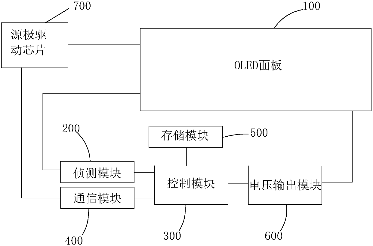
[0042] The present invention provides an AMOLED display device, please refer to image 3 , is a schematic structural diagram of the first embodiment of the AMOLED display device of the present invention, the AMOLED display device of the present invention includes an OLED panel 100, a detection module 200 electrically connected to the OLED panel 100, and a detection module 200 electrically connected The control module 300 , the communication module 400 electrically connected to the control module 300 , the storage module 500 electrically connected to the control module 300 , and the voltage output module 600 electrically connected to the control module 300 and the OLED panel 100 .

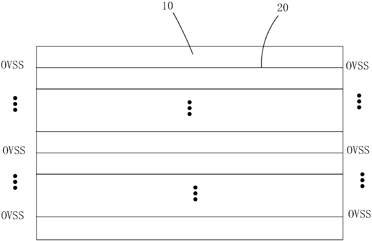
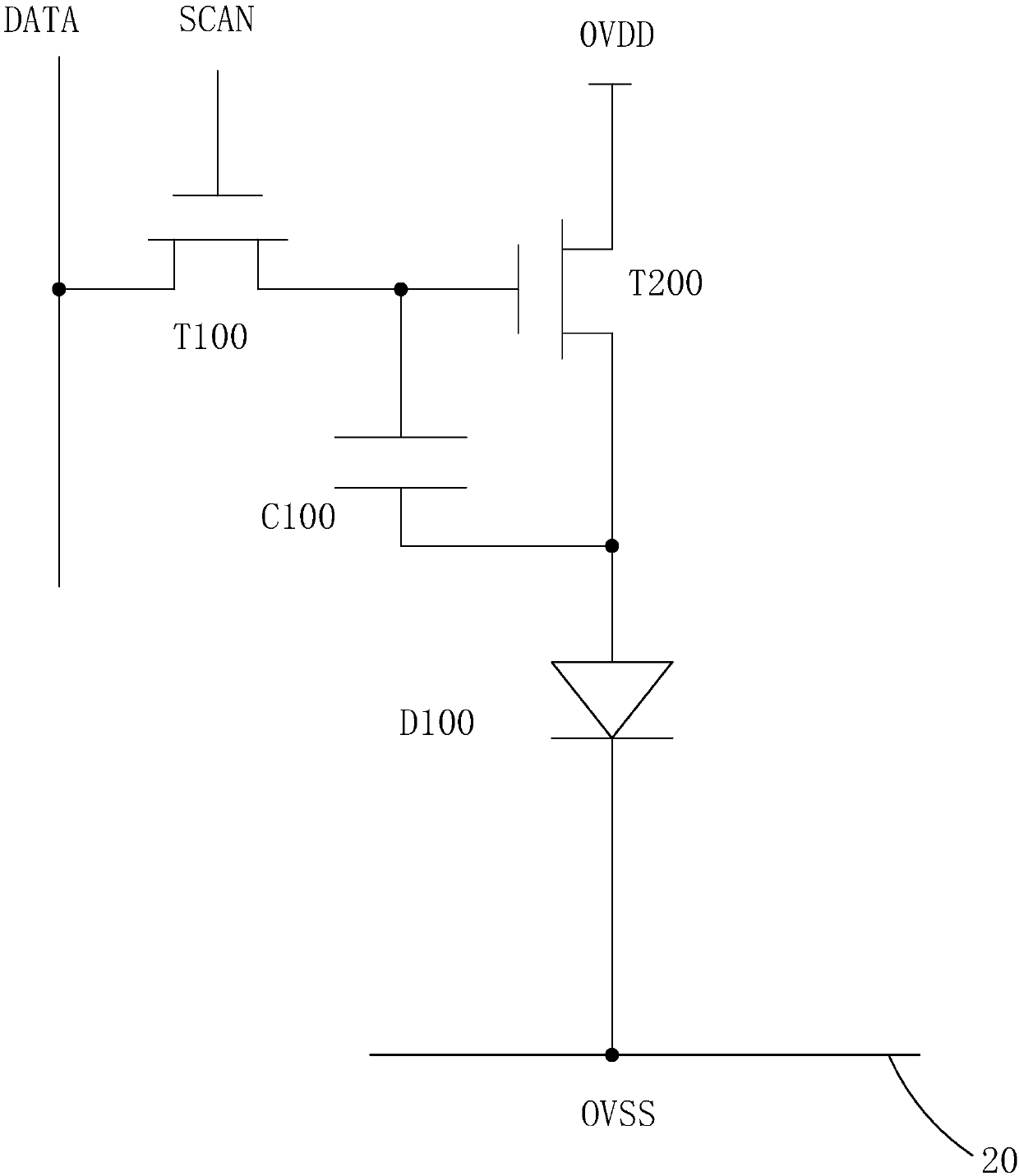
[0043] Among them, see Figure 4 , the OLED panel 100 include...


PUM


Abstract

The present invention provides an AMOLED display device and a driving method thereof. The OLED panel of the AMOLED display device of the present invention has a plurality of sub pixels. Each row of sub pixels is correspondingly and electrically connected to an OVSS routing, and at least one sub pixel in a substrate center area is a detection sub pixel. In driving, a detection module is used to obtain a maximum value of power negative voltage inputted into the detection sub pixel, a communication module receives a highest gray level value or highest data signal voltage in a picture which needsto be displayed, a control module searches in a look-up table stored in a memory module to obtain corresponding minimum power positive voltage according to the highest gray level value or highest datasignal voltage in the picture which needs to be displayed and the maximum value of the power negative voltage inputted into the detection sub pixel and generates a corresponding control signal to control a voltage output module to output corresponding power positive voltage to the OLED panel. The display power consumption of the AMOLED display device can be reduced, and the display quality of theAMOLED display device is improved at the same time.

Description

technical field [0001] The present invention relates to the field of display technology, in particular to an AMOLED display device and a driving method thereof. Background technique [0002] Organic light emitting diode (Organic Light Emitting Display, OLED) display device has self-illumination, low driving voltage, high luminous efficiency, short response time, high definition and contrast, nearly 180° viewing angle, wide operating temperature range, and can realize flexible display and With many advantages such as large-area full-color display, it is recognized by the industry as a display device with the most potential for development. [0003] According to the driving mode, OLEDs can be divided into two types: passive driving and active driving, that is, direct addressing and thin film transistor (Thin Film Transistor, TFT) matrix addressing. Among them, active driving is also called active matrix (ActiveMatrix, AM) type, and each light emitting unit in the AMOLED is in...

Claims


Application Information

Patent Timeline
Patent Type & Authority Applications(China)
IPC IPC(8): G09G3/3225
CPCG09G3/3225G09G3/3233G09G2330/028G09G2320/0295H10K59/12G09G3/3258G09G3/3266G09G3/3275G09G2300/0819G09G2310/08G09G2300/0439G09G2330/021H10K50/81H10K50/82H10K59/131
Inventor 王振岭
Owner SHENZHEN CHINA STAR OPTOELECTRONICS SEMICON DISPLAY TECH CO LTD
Why Eureka
Try Eureka