Array substrate, preparation method thereof and liquid crystal panel

An array substrate and substrate substrate technology, which is applied in semiconductor/solid-state device manufacturing, optics, instruments, etc., can solve the problems of low utilization efficiency of backlight sources, and achieve the effects of easy operation, simple preparation process, and reduced production costs.

Inactive Publication Date: 2017-11-07
TUNGHSU KUNSHAN DISPLAY MATERIAL CO LTD +2
View PDF3 Cites 3 Cited by
  • Summary
  • Abstract
  • Description
  • Claims
  • Application Information

AI Technical Summary

Problems solved by technology

[0004] The object of the present invention is to provide an array substrate capable of reflecting the light passing through the grid to overcome the problem of low utilization

Method used


Image

  • Array substrate, preparation method thereof and liquid crystal panel

Examples


Embodiment Construction

[0029] In the present invention, unless stated to the contrary, the used orientation words such as "up, down, left, and right" usually refer to the orientations shown in the drawings and the orientations in practical applications.

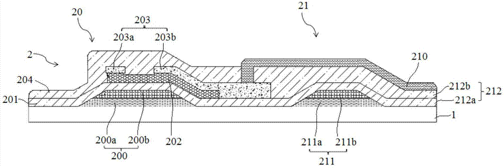
[0030] The present invention provides an array substrate, which includes a base substrate 1, a plurality of pixel units 2 formed on the base substrate 1 and distributed in an array, each pixel unit 2 includes a thin film transistor switch 20, wherein , the thin film transistor switch 20 includes a grid 200 formed on the base substrate 1, the grid 200 includes a first reflective layer 200a formed on the base substrate 1, and the grid 200 can reflect back the light passing through the grid 200 itself . By setting the grid 200 containing the first reflective layer 200a on the base substrate 1, so that when the light emitted by the backlight passes through the array substrate, the grid 200 can reflect back the light passing through itself, so that when...


PUM

PropertyMeasurementUnit
Thicknessaaaaaaaaaa
Thicknessaaaaaaaaaa

Abstract

The invention relates to the field of liquid crystal display and discloses an array substrate, a preparation method thereof and a liquid crystal panel. The array substrate comprises a substrate body (1) and multiple pixel units (2) formed on the substrate body (1) in array distribution, and each pixel unit comprises a thin film transistor switch (20) which comprises a grid electrode (200) formed on the substrate body (1). The array substrate can reflect back light going through the grid electrodes, so that utilization efficiency of a backlight source is improved. A mask is used for few times in the preparation method, so that the preparation method is convenient to operate, and production cost is lowered. By applying the array substrate or the array substrate prepared by the preparation method in the liquid crystal panel, the utilization efficiency of the backlight source can be improved, and display power consumption of the liquid crystal panel is lowered.

Description

technical field [0001] The invention relates to liquid crystal display technology, in particular to an array substrate, a preparation method of the array substrate and a liquid crystal panel. Background technique [0002] Among the flat panel displays, Thin Film Transistor Liquid Crystal Display (TFT-LCD) has the characteristics of small size, no radiation and relatively low manufacturing cost, and occupies a dominant position in the current flat panel display market. TFT-LCD generally includes a liquid crystal panel and a backlight module (also called a backlight). The LCD panel itself does not emit light, it displays graphics or characters that are the result of its light modulation. The backlight module is one of the key components of TFT-LCD. It is a light source located behind the thin-film transistor liquid crystal display. It can provide a uniform and high-brightness light source for the liquid crystal panel, so that the TFT-LCD can display images normally. The back...

Claims


Application Information

Patent Timeline
IPC IPC(8): G02F1/1368G02F1/1335H01L27/12H01L21/77
CPCG02F1/133553G02F1/1368G02F1/136295H01L27/1214H01L27/1259
Inventor 向长江
Owner TUNGHSU KUNSHAN DISPLAY MATERIAL CO LTD
Why Eureka
Try Eureka