

Thin film package body and display panel
A thin-film packaging and display panel technology, which is applied in the fields of electric solid-state devices, semiconductor devices, semiconductor/solid-state device manufacturing, etc., can solve the problems of weak resistance to water and oxygen and bending resistance
- Summary
- Abstract
- Description
- Claims
- Application Information
AI Technical Summary
Problems solved by technology
Method used
Image

Examples
Embodiment Construction
[0021] In order for those skilled in the art to better understand the technical solution of the present application, a thin film packaging body, a display panel and a thin film packaging method provided by the invention will be further described in detail below with reference to the accompanying drawings and specific embodiments.
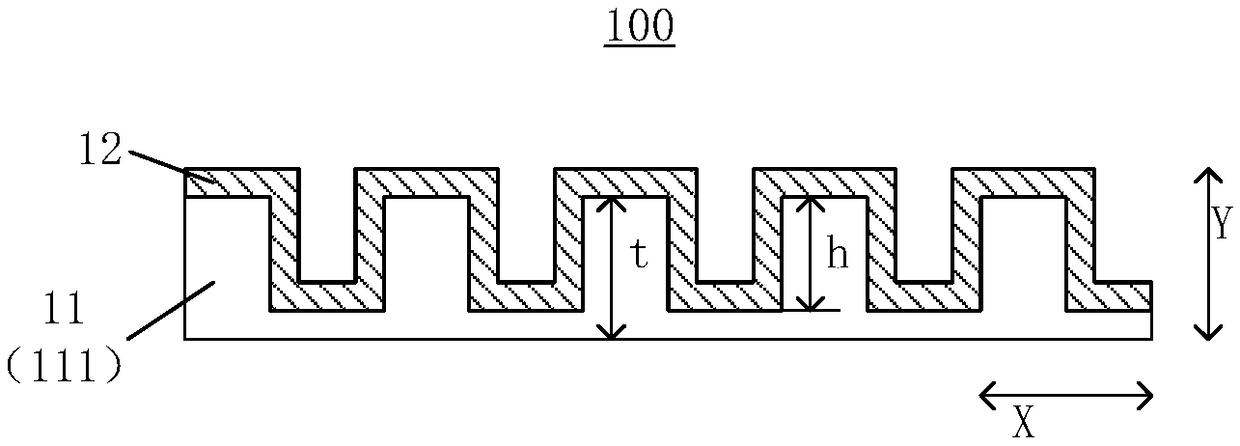
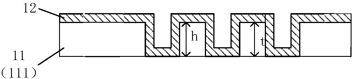
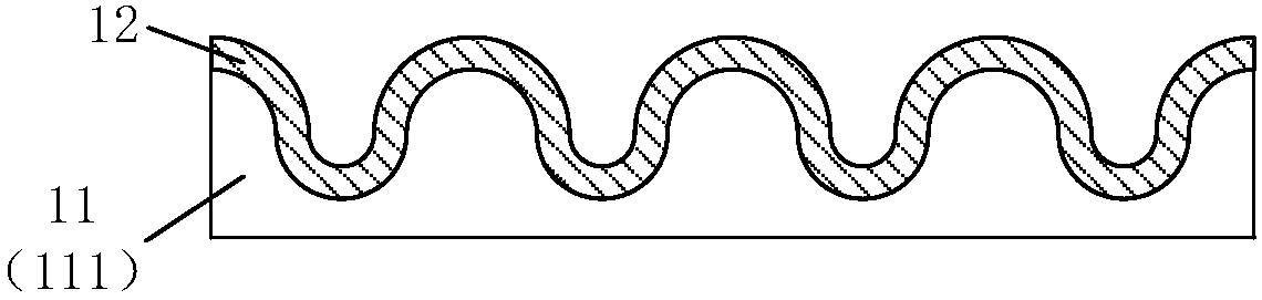
[0022] see Figure 1-3 , figure 1 It is a structural schematic diagram of the first embodiment of the thin film packaging body of the present application, figure 2 Yes figure 1 A schematic diagram of a first possible shape of the first embodiment of the thin film encapsulation shown, image 3 Yes figure 1 Schematic illustration of a second possible shape for the first embodiment of the thin film encapsulation shown.
[0023] The thin film package 100 of this embodiment includes a substrate layer 11 and an inorganic conformal layer 12 . The substrate layer 11 includes at least one organic substrate layer 111, at least part of one side of the or...
PUM
 Abstract
Description
Claims
Application Information