A packaging structure for a direct-lit backlight source and a manufacturing method thereof
A technology of encapsulation structure and manufacturing method, which is applied in optics, nonlinear optics, instruments, etc., can solve problems such as water and oxygen infiltration at the edge, degradation of quantum dot luminous performance, and failure to consider luminous efficiency, etc., to achieve complete structure and function, Good water and oxygen barrier ability, good light guide effect
- Summary
- Abstract
- Description
- Claims
- Application Information
AI Technical Summary
Problems solved by technology
Method used
Image
Examples
Embodiment 1
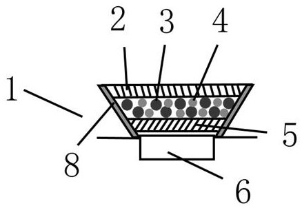
[0032] figure 1 It shows the packaging structure for direct type quantum dot backlight, which includes substrate layer 1, barrier layer 2, red quantum dots 3, green quantum dots 4, packaging layer 5, blue light source 6, optical film 7 , reflective layer 8 . exist figure 1 In the first basic structure shown in , the quantum dot microstructure array dimming layer is composed of quantum dots and composite materials. The quantum dot microstructure array contains one or more quantum dots and composite materials with a central wavelength between 380-780nm. It is made of quantum dot slurry by mixing quantum dots and composite materials in a certain proportion. Depending on requirements, the quantum dot microstructure array is formed by methods such as inkjet printing, and the thickness of the quantum dot microstructure array is 20-50 μm. Outside the dimming layer of the quantum dot microstructure array is the encapsulation layer, which is made of inorganic materials such as silic...
Embodiment 2
[0039] Figure 4 It shows the packaging structure for direct type quantum dot backlight, which includes substrate layer 1, barrier layer 2, red quantum dots 3, green quantum dots 4, packaging layer 5, blue light source 6, optical film 7 , reflective layer 8 . Figure 4 On the basis of Embodiment 1, grooves are formed on the lower surface of the substrate by methods such as photolithography, erosion or laser etching. The quantum dot microstructure array dimming layer is composed of quantum dots and composite materials. The configuration and formation of the quantum dot microstructure array are similar to those in Embodiment 1 of the present invention, and will not be repeated here. The only difference is that after the groove is formed, the inclined walls on both sides inside the groove are coated with high reflectivity materials by spraying, evaporation, etc., so that the light of the direct light source can all be emitted from the microstructure, and has a certain Directivi...
PUM
| Property | Measurement | Unit |
|---|---|---|
| surface tension | aaaaa | aaaaa |
| particle size | aaaaa | aaaaa |
| thickness | aaaaa | aaaaa |
Abstract
Description
Claims
Application Information


