

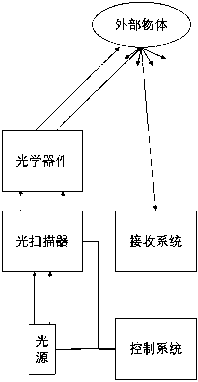
Photoelectric scanner
A technology of optical devices and light sources, applied in the optical field, can solve the problems of the exit angle and exit position of unseen light, and achieve the effect of improving quality
- Summary
- Abstract
- Description
- Claims
- Application Information
AI Technical Summary
Problems solved by technology
Method used
Image

Examples
Embodiment 1
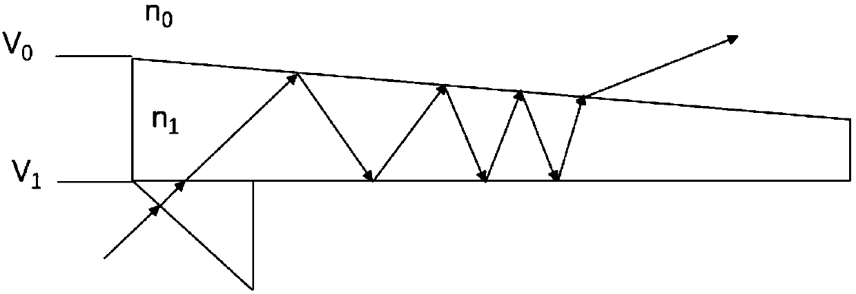
[0040] According to an optical scanning device provided by the present invention, the purpose of beam scanning is realized by changing the effective refractive index of the birefringent medium in the device and changing the angle and / or position of outgoing light. The device may be a waveguide device whose cross-sectional shape is triangular or wedge-shaped. It has at least two surfaces, and the two surfaces are not parallel. The substrate on the surface can apply voltage, and the middle is filled with a birefringent material (such as liquid crystal). When the electric field of the substrates at both ends changes, the equivalent refractive index of the middle material will also change. Changes occur, thereby changing the outgoing direction and / or position of the incident light beam to realize scanning. Applying a voltage to change the refractive index of the material can be achieved by two methods or their combination (ie, two driving methods and their combination).
[0041] ...
Embodiment 2
[0049]A device for optical scanning, which is a wedge-shaped waveguide. The upper substrate and the lower substrate (referred to as the upper and lower substrates) use ITO glass. The upper and lower substrates are not parallel and are equipped with electrodes. A PI film is prepared on the inner side of the substrate, which is aligned and positioned by the rubbing method (use a felt to rub the PI film on the glass substrate in a specific direction), the alignment directions of the upper and lower substrates are consistent (ECB mode), and the four sides are sealed and filled in the middle liquid crystal material. A triangular prism made of a material with the same or similar refractive index is glued on the lower substrate of the device with optical glue having the same or similar refractive index as the lower substrate, and the incident light is guided into the waveguide through the triangular prism. The light source uses semiconductor lasers, such as 808nm or 1550nm lasers, an...
PUM
 Abstract
Description
Claims
Application Information