Silicon wafer processing device and method
A technology for processing devices and silicon wafers, which is applied in the direction of photolithography exposure devices, microlithography exposure equipment, instruments, etc., and can solve the problems of expensive equipment and inability to achieve full-coverage exposure of silicon wafers
- Summary
- Abstract
- Description
- Claims
- Application Information
AI Technical Summary
Problems solved by technology
Method used
Image

Examples
Embodiment Construction
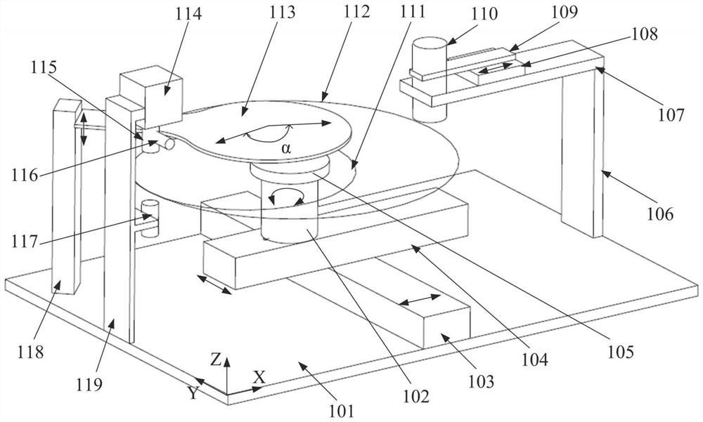
[0049] The specific implementation manner of the present invention will be described in more detail below with reference to schematic diagrams. Advantages and features of the present invention will be apparent from the following description and claims. It should be noted that all the drawings are in a very simplified form and use imprecise scales, and are only used to facilitate and clearly assist the purpose of illustrating the embodiments of the present invention.
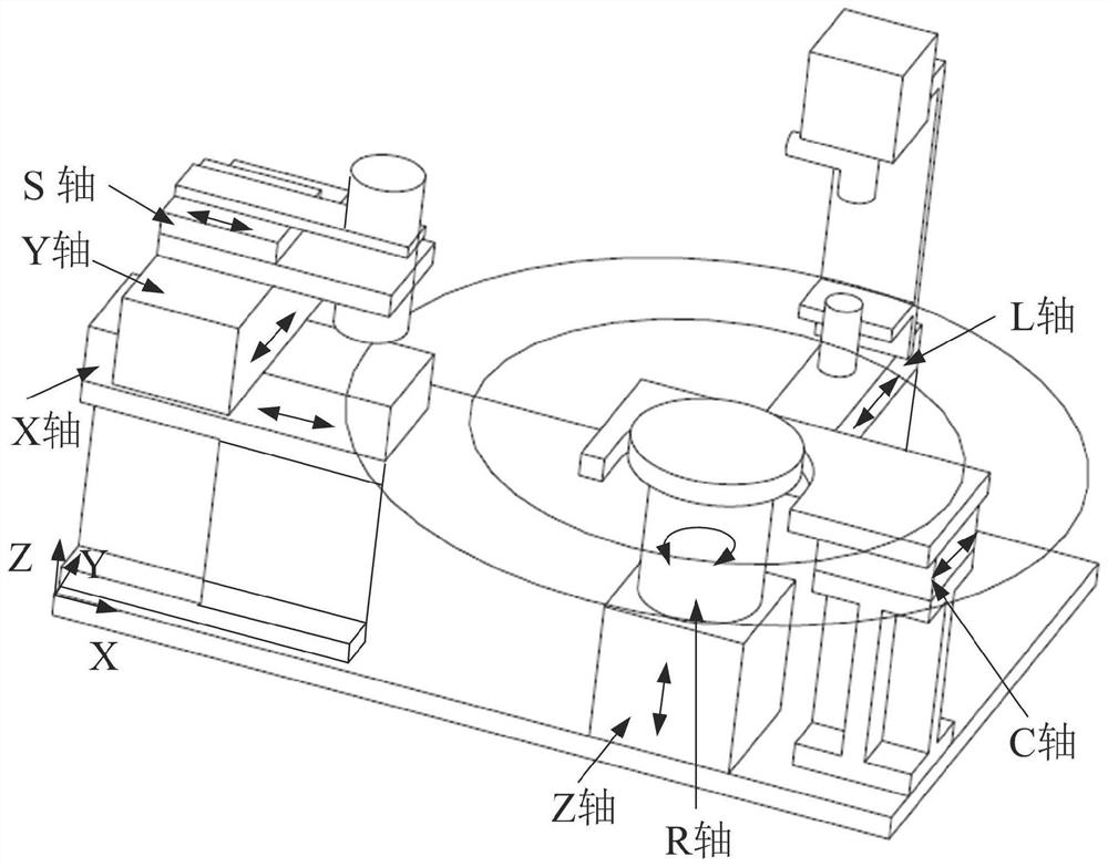
[0050] As mentioned in the background art, the requirements for pre-alignment and edge exposure in the market are getting higher and higher, and the degree of automation is getting higher and higher. For the pre-alignment function, it is not only required to be able to complete the pre-alignment of various types of process wafers, but also to realize the processing of 8-inch and 12-inch silicon wafers at the same time. For the edge exposure function, it is not only required to realize edge exposure, multiple exp...
PUM
| Property | Measurement | Unit |
|---|---|---|
| thickness | aaaaa | aaaaa |
| size | aaaaa | aaaaa |
Abstract
Description
Claims
Application Information
 - R&D Engineer
- R&D Manager
- IP Professional
- Industry Leading Data Capabilities
- Powerful AI technology
- Patent DNA Extraction
Browse by: Latest US Patents, China's latest patents, Technical Efficacy Thesaurus, Application Domain, Technology Topic.
© 2024 PatSnap. All rights reserved.Legal|Privacy policy|Modern Slavery Act Transparency Statement|Sitemap