
Broadband wave-absorbing frequency selection surface
A technology for selecting the surface and wave frequency, applied in the field of electromagnetic metamaterials, can solve the problems of limited practical application, high surface quality and density, large volume, etc., and achieve the effect of simple structure, easy processing, and good angular stability
Patent Information
- Authority / Receiving Office
- CN · China
- Current Assignee / Owner
- Publication Date
- 2019-08-23
Smart Images
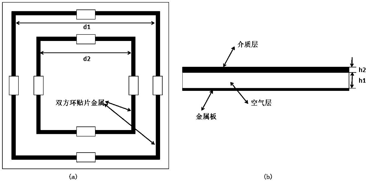
Figure 1 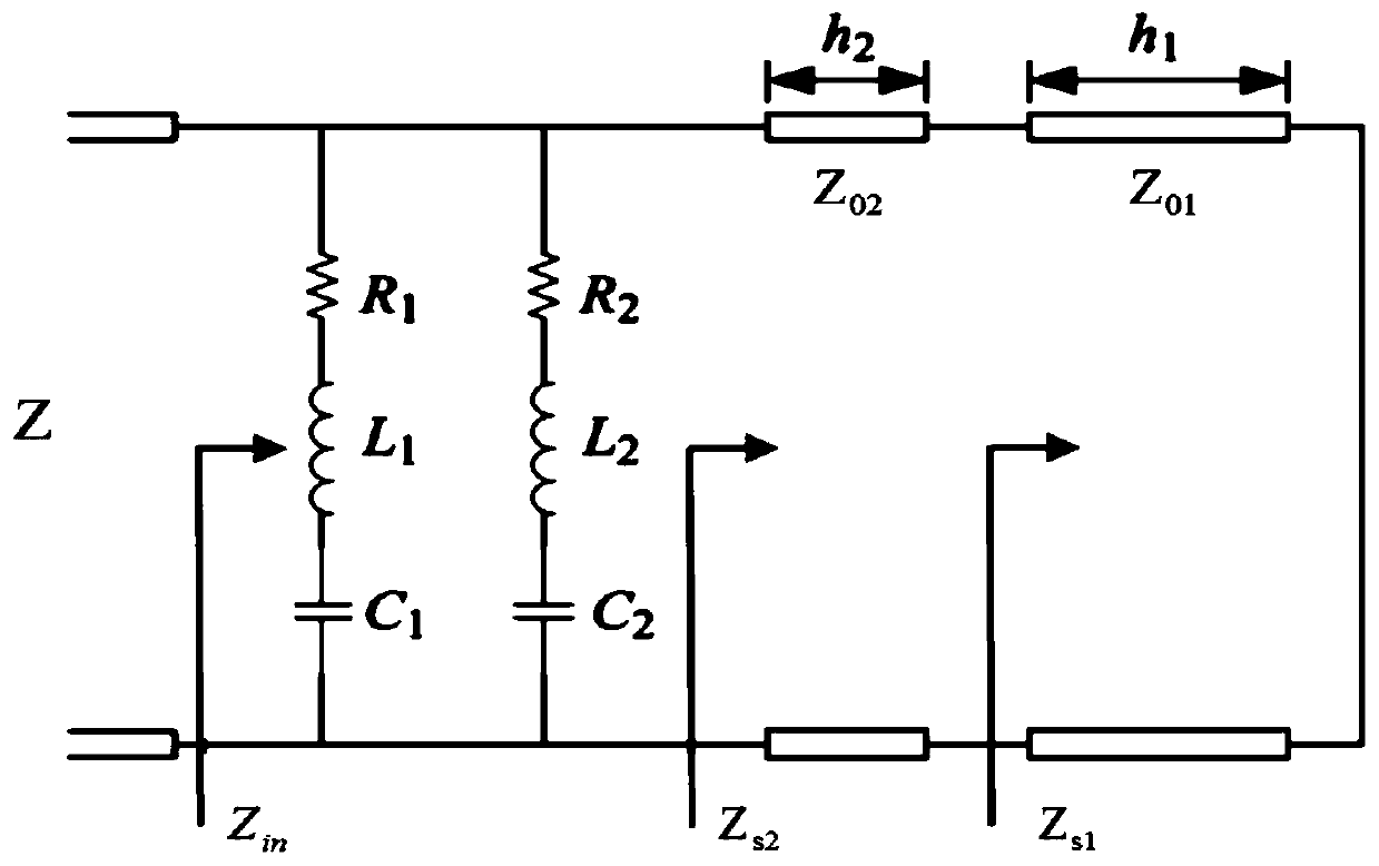
Figure 2 
Figure 3
Abstract
Description
technical field
[0001] The invention belongs to the technical field of electromagnetic metamaterials, and in particular relates to a frequency selective surface. Background technique
[0002] Frequency Selective Surface (FSS) is composed of periodically arranged metal patches or gaps, which has good spatial filtering characteristics and can reflect out-of-band electromagnetic waves while transmitting in-band electromagnetic waves.
[0003] Electromagnetic wave absorbers can be used to reduce the radar scattering cross-sectional area and realize radar stealth. Microwave absorber design requires wide bandwidth and small thickness. The earliest wave absorber, the Salisbury screen, consists of a resistive film, a dielectric, and a metal bottom plate. When the thickness of the medium is a quarter of the wavelength, the free space matches the impedance of the absorber to produce a wave-absorbing effect. However, this absorber has a narrow absorption bandwidth and a thicker thic...
Examples
Embodiment Construction
[0017] The technical solutions of the present invention will be described in detail below in conjunction with the accompanying drawings.
[0018] Such as figure 1 As shown, the broadband wave-absorbing frequency selective surface designed by the present invention includes upper and lower layers of dielectric plates, an air layer is between the two layers of dielectric plates, and the surface of the upper layer of dielectric plates is provided with two ring metal patches arranged periodically, each A square ring metal patch is loaded with a resistor, and the lower dielectric board is a metal plate. Preferably, a resistor is connected in series at the midpoint of each side of each square ring metal patch.
[0019] figure 2 Equivalent circuit diagram of the broadband absorbing frequency selective surface designed for the present invention. Each square ring in the two rings is equivalent to a capacitor (C in the figure 1 、C 2 ), inductance (L 1 , L 2 ) and resistance (R 1...