A kind of array substrate and preparation method thereof

An array substrate and substrate technology, applied in the field of array substrate and its preparation, can solve the problems of poor antistatic ability of display panel, complicated array substrate process, high production cost, etc. simple effect

Active Publication Date: 2021-09-03
TCL CHINA STAR OPTOELECTRONICS TECH CO LTD
View PDF0 Cites 0 Cited by
  • Summary
  • Abstract
  • Description
  • Claims
  • Application Information

AI Technical Summary

Problems solved by technology

[0007] The purpose of the present invention is to provide an array substrate and its preparation method to solve the problems in the prior art that the GOA circuit space is compressed to realize the narrow frame of the display panel, which will cause poor antistatic ability of the display panel, and the problems in the prior art The technical problems of complex process and high production cost for preparing array substrates

Method used


Image

  • A kind of array substrate and preparation method thereof
  • A kind of array substrate and preparation method thereof
  • A kind of array substrate and preparation method thereof

Examples


Embodiment Construction

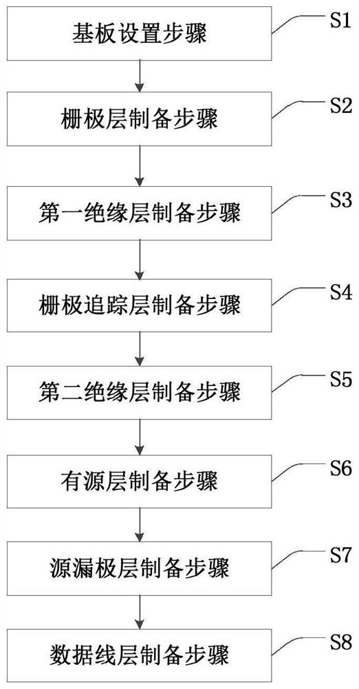
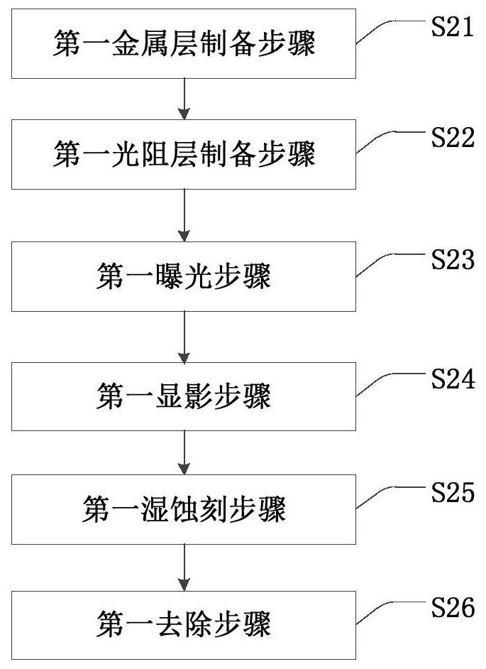
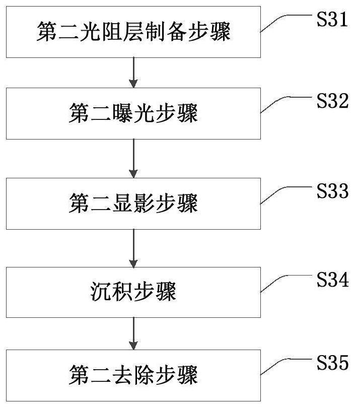
[0036] The preferred embodiments of the present invention are introduced below with reference to the accompanying drawings, in order to prove that the present invention can be implemented, and these embodiments can completely introduce the technical content of the present invention to those skilled in the art, so that the technical content of the present invention is more clear and easy to understand. However, the present invention can be embodied in many different forms of embodiments, and the protection scope of the present invention is not limited to the embodiments mentioned herein.

[0037]The terms "first", "second", etc. (if any) in the description and claims of the present invention and the above drawings are used to distinguish similar objects and not necessarily to describe a specific order or sequence. It should be understood that the items so described are interchangeable under appropriate circumstances. Furthermore, the terms "comprising" and "having", as well as...


PUM


Abstract

The present invention provides an array substrate and a preparation method thereof. The array substrate includes a substrate, a gate layer, a first insulating layer, a gate tracking layer, and a second insulation layer; the preparation method of the array substrate includes a substrate setting step, The gate layer preparation step, the first insulating layer preparation step, the gate tracking layer preparation step and the second insulating layer preparation step; the invention provides an array substrate and its preparation method, one end of the gate tracking layer is directly connected through a through hole To the gate layer, the other end is connected to the IC circuit in the non-display area, wherein the gate trace layer is set in the display area, reducing the wiring space in the non-display area, so that the display panel can achieve the effect of narrow borders. In addition, the gate When the tracking layer is in contact with the grid layer, the contact resistance between the grid tracking layer and the grid layer can be reduced, and the preparation process of the array substrate is simple.

Description

technical field [0001] The present invention relates to the field of display technology, in particular to an array substrate and a preparation method thereof. Background technique [0002] At present, narrow bezel or even bezel-less screens have become the mainstream direction of small-sized mobile phones in the current market. In order to increase the screen ratio as much as possible and realize narrow bezels or even bezel-less mobile phone screens, it is necessary to reduce the left and right edges and the upper and lower edges as much as possible. . [0003] GOA technology (Gate Driver on Array) is the array substrate line drive technology. It uses the original array process of the liquid crystal display panel to manufacture the drive circuit of the horizontal scanning line on the substrate around the display area, so that it can replace the external integrated circuit board ( Integrated Circuit, IC) to complete the drive of the horizontal scanning line. GOA technology ...

Claims


Application Information

Patent Timeline
Patent Type & Authority Patents(China)
IPC IPC(8): G02F1/1362G02F1/1368
CPCG02F1/136204G02F1/136286G02F1/1368
Inventor 夏慧
Owner TCL CHINA STAR OPTOELECTRONICS TECH CO LTD
Why Eureka
Try Eureka