Substrate, preparation method thereof and display device

A technology for display devices and substrates, which can be used in semiconductor/solid-state device manufacturing, instruments, semiconductor devices, etc., and can solve problems such as poor contact between the first conductive layer and the second conductive layer.

Active Publication Date: 2020-08-07
HEFEI XINSHENG OPTOELECTRONICS TECH CO LTD +1
View PDF5 Cites 5 Cited by
  • Summary
  • Abstract
  • Description
  • Claims
  • Application Information

AI Technical Summary

Problems solved by technology

[0003] Embodiments of the present application provide a substrate and its preparation method, and a display device, which can solve the problem of poor contact between the first conductive layer and the second conductive layer

Method used


Image

  • Substrate, preparation method thereof and display device
  • Substrate, preparation method thereof and display device
  • Substrate, preparation method thereof and display device

Examples


Embodiment Construction

[0043] The following will clearly and completely describe the technical solutions in the embodiments of the application with reference to the drawings in the embodiments of the application. Apparently, the described embodiments are only some of the embodiments of the application, not all of them. Based on the embodiments in this application, all other embodiments obtained by persons of ordinary skill in the art without making creative efforts belong to the scope of protection of this application.

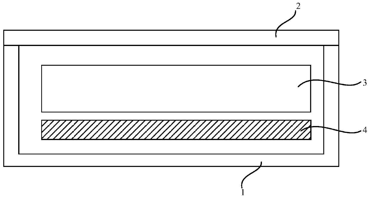
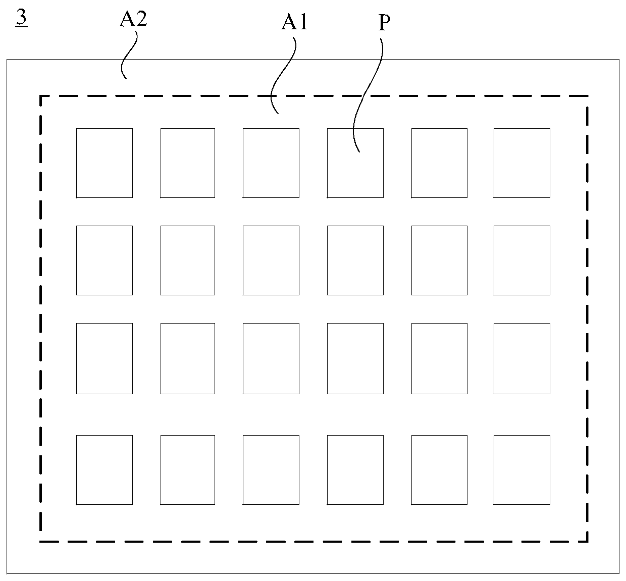
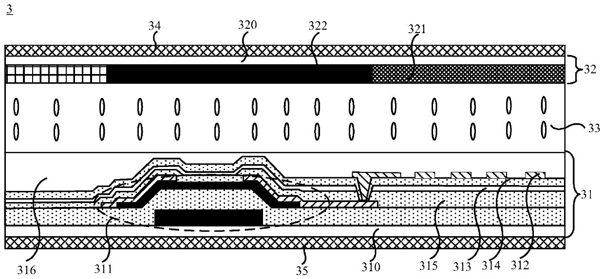
[0044] An embodiment of the present invention provides a display device. The type of the display device is not limited, and may be a liquid crystal display (Liquid Crystal Display, LCD for short), or an electroluminescent display device. In the case that the display device is an electroluminescent display device, the electroluminescent display device may be an organic electroluminescent display device (Organic Light-Emitting Diode, OLED for short) or a quantum dot electroluminescent ...


PUM


Abstract

The embodiment of the invention provides a substrate, a preparation method thereof and a display device, relating to the technical field of the display. The problem of poor contact between a first conductive layer and a second conductive layer can be solved; the substrate comprises a first conductive layer arranged on a substrate body, conductive protrusions arranged on the surface of the side, away from the substrate body, of the first conductive layer and a dielectric layer covering the first conductive layer, the conductive protrusions and the substrate body, and first via holes are formedin the positions, corresponding to the conductive protrusions, of the dielectric layer. The substrate further comprises a second conductive layer which is arranged on the surface of the side, away from the substrate body, of the dielectric layer and electrically connected with the conductive protrusions through the first via holes.

Description

technical field [0001] The present application relates to the field of display technology, in particular to a substrate, a manufacturing method thereof, and a display device. Background technique [0002] A top-gate TFT (Thin Film Transistor, thin film transistor) has the characteristics of a short channel, so its on-state current Ion can be effectively increased, so that the display effect can be significantly improved and power consumption can be effectively reduced. Moreover, the overlapping area between the gate and the source and drain of the top-gate TFT is small, so the parasitic capacitance can be effectively reduced, and the refresh frequency is higher. Therefore, the top-gate TFT is an important research direction at present. Contents of the invention [0003] Embodiments of the present application provide a substrate, a manufacturing method thereof, and a display device, which can solve the problem of poor contact between the first conductive layer and the seco...

Claims


Application Information

Patent Timeline
Patent Type & Authority Applications(China)
IPC IPC(8): H01L27/12H01L21/77H01L27/32G02F1/1362G02F1/1368
CPCH01L27/124H01L27/1259H01L21/77G02F1/1362G02F1/136227G02F1/1368H01L2021/775H10K59/131
Inventor 宋威赵策刘宁刘军王庆贺丁远奎程磊磊倪柳松
Owner HEFEI XINSHENG OPTOELECTRONICS TECH CO LTD
Why Eureka
Try Eureka