Miniature memory packaging structure and memory packaging structure

A packaging structure and memory technology, applied in the directions of antenna supports/installation devices, electric solid devices, semiconductor devices, etc., can solve the problems of increasing material costs, large wiring space, etc., reducing manufacturing costs, increasing wiring space, The effect of reducing the line space

Pending Publication Date: 2021-03-05
CHIPMOS TECH INC
View PDF0 Cites 0 Cited by
  • Summary
  • Abstract
  • Description
  • Claims
  • Application Information

AI Technical Summary

Problems solved by technology

Generally speaking, wire bonding is usually used for packaging. However, since this type of packaging requires more bonding

Method used


Image

  • Miniature memory packaging structure and memory packaging structure
  • Miniature memory packaging structure and memory packaging structure
  • Miniature memory packaging structure and memory packaging structure

Examples


Example Embodiment

[0037] The present invention will be described more fully with reference to the accompanying drawings of this embodiment. However, the present invention can also be embodied in various forms and should not be limited to the embodiments described herein. The thickness, size or size of layers or regions in the drawings may be exaggerated for clarity. The same or similar reference numerals denote the same or similar elements, and the following paragraphs will not repeat them one by one.

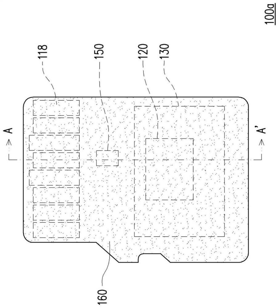
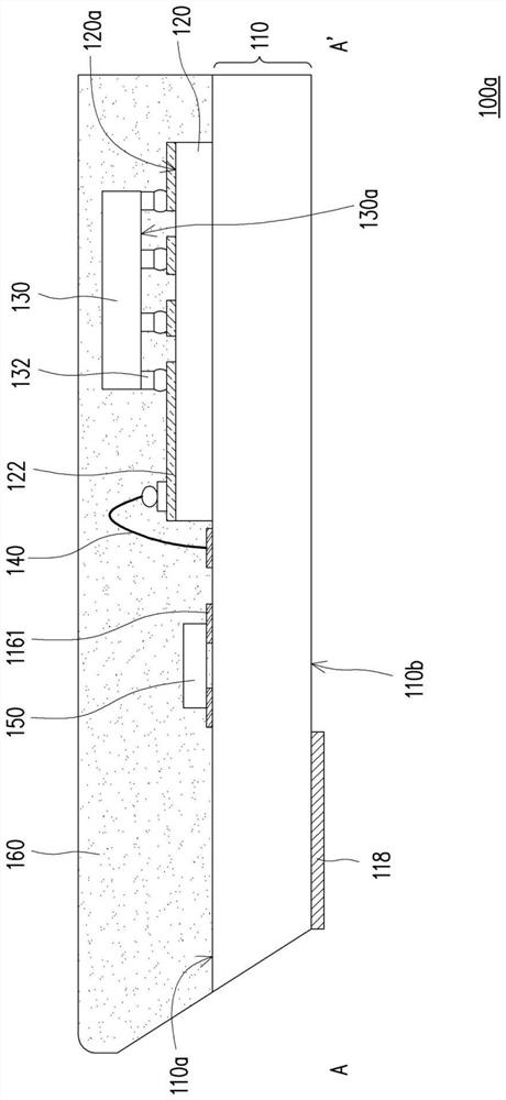
[0038] Figure 1A is a schematic top view of a memory package structure according to an embodiment of the present invention. Figure 1B Yes Figure 1A Schematic cross-sectional view along section line A-A'. In this embodiment, the size of the micro memory package structure 100a may conform to the size of a micro secure digital memory card (Micro Secure Digital, Micro SD).

[0039] Please also refer to Figure 1A and Figure 1B , in this embodiment, the micro memory package structure 100 a in...


PUM


Abstract

The invention provides a miniature memory packaging structure. The miniature memory packaging structure comprises a circuit substrate, a first chip, a second chip and a packaging colloid, the circuitsubstrate is provided with a first surface, a second surface opposite to the first surface and a conductive pattern located on the second surface. The first chip is disposed on the first surface. Thefirst chip is provided with a first active surface far away from the first surface and a redistribution circuit layer located on the first active surface, and the redistribution circuit layer is electrically connected with the circuit substrate. The second chip is disposed on the first active surface and electrically connected to the redistribution layer. The second chip has a second active surface facing the first active surface. The packaging colloid is disposed on the first surface and covers the first chip and the second chip. The invention further provides a memory packaging structure with a antenna.

Description

technical field [0001] The invention relates to a memory package structure, in particular to a micro memory package structure and a memory package structure. Background technique [0002] With the vigorous development of the electronic industry, electronic products are also developing in the direction of lightness, thinness, shortness, smallness, high density and multi-function. Generally speaking, wire bonding is usually used for packaging. However, since this type of packaging requires more bonding wires (such as gold wires), a large space for bonding wires needs to be reserved. Many material costs will be increased. Therefore, how to reduce the overall size and reduce the production cost will become an important subject. Contents of the invention [0003] The invention provides a micro memory packaging structure, which can reduce the overall size and reduce the manufacturing cost. [0004] The invention provides a memory package structure integrated with an antenna. ...

Claims


Application Information

Patent Timeline
IPC IPC(8): H01L25/07H01L25/00H01L23/58H01L23/498H01L25/18H01Q1/22
CPCH01L25/072H01L25/071H01L25/50H01L25/18H01L23/58H01L23/49838H01Q1/2283H01L2224/16145H01L2224/48091H01L2924/181H01L2924/00014H01L2924/00012
Inventor 卢东宝徐子涵齐中邦张家豪
Owner CHIPMOS TECH INC
Why Eureka
Try Eureka