Display device

A display device and pixel technology, which is applied to static indicators, instruments, electrical components, etc., can solve the problems of shortening the charging time of thin-film transistors and making the driving voltage of thin-film transistors difficult, so as to ensure charging time and wide driving voltage range , the effect of delayed reaction time

Pending Publication Date: 2021-12-17
SAMSUNG DISPLAY CO LTD
View PDF0 Cites 0 Cited by
  • Summary
  • Abstract
  • Description
  • Claims
  • Application Information

AI Technical Summary

Problems solved by technology

[0003] However, as the driving frequency of the display device increases or the resolution increases, it becomes difficult to ensure the driving voltage of the thin film transistor, and there may be a problem that the time for charging the thin film transistor becomes shorter.

Method used


Image

  • Display device
  • Display device
  • Display device

Examples


Embodiment Construction

[0049] Hereinafter, embodiments of the present invention will be described in more detail with reference to the attached drawings. The same reference numerals are used for the same components in the drawings, and repeated descriptions of the same components are omitted.

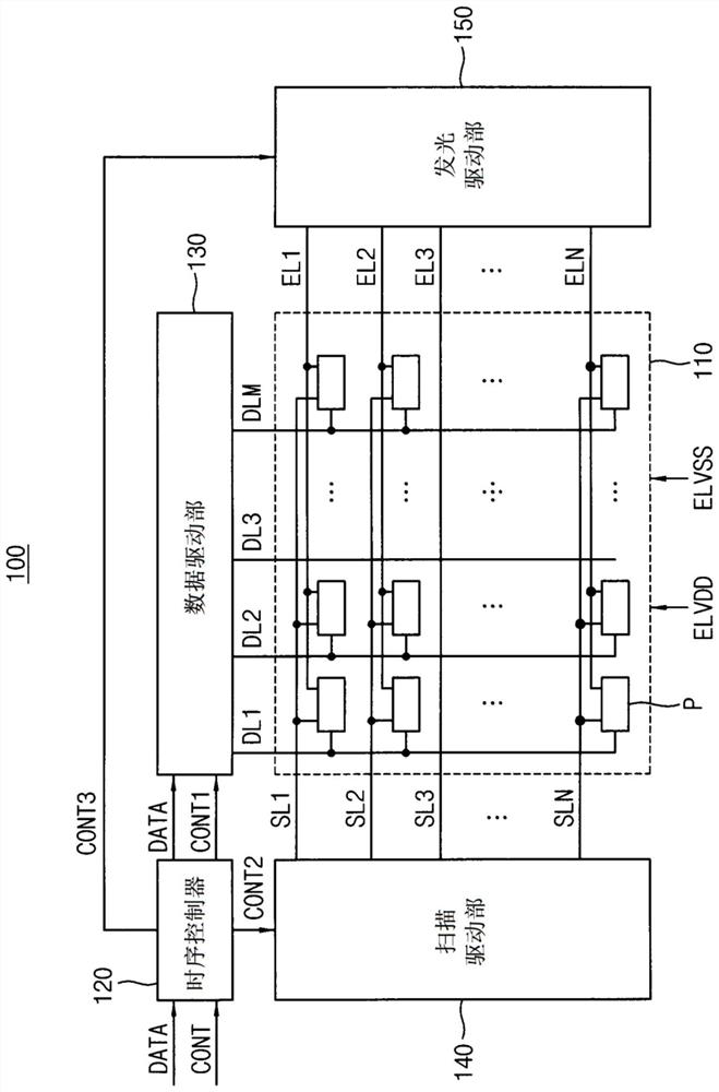
[0050] figure 1 is a block diagram showing a display device according to an embodiment of the present invention.

[0051] refer to figure 1 , the display device 100 may include a display unit 110 , a timing controller 120 , a data driving unit 130 , a scanning driving unit 140 and a light emitting driving unit 150 .

[0052] The display unit 110 may include a plurality of pixels P. Referring to FIG. The plurality of pixels P may be connected to a plurality of scan lines SL1, . . . , SLN, a plurality of data lines DL1, .

[0053] The data lines DL1 , . The scan lines SL1 , . The light emission control lines EL1 , .

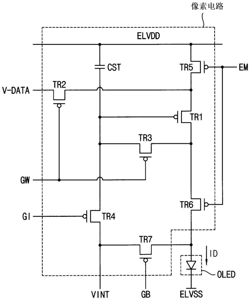
[0054] The pixel P may receive a first power supply voltage ELVDD and a second power su...


PUM


Abstract

The invention discloses a display device which includes a pixel including a pixel driving transistor and a pixel switching transistor, the pixel driving transistor including a first active layer including a first channel area having a first length, a first gate insulating layer on the first active layer, a first gate electrode on the first gate insulating layer, a first source electrode above the first gate electrode and connected to a source area of the first active layer, and a first drain electrode connected to a drain area of the first active layer; wherein the pixel switching transistor comprises: a second active layer comprising a second channel area having a second length that is shorter than the first length, a second gate insulating layer on the second active layer, a second gate electrode on the second gate insulating layer, a second source electrode above the second gate electrode and connected to a source area of the second active layer, and a second drain electrode above the second gate electrode and connected to a drain area of the second active layer.

Description

technical field [0001] The present invention relates to a display device, and more particularly to a display device including a plurality of transistors. Background technique [0002] Along with the miniaturization of display devices, in order to increase the size of the display area, efforts are being made to minimize the peripheral portion of the display area, that is, the bezel area. In general, since wiring for driving a display device and driving circuits are arranged in a frame area corresponding to a non-display area, there is a limitation in minimizing the frame area. Therefore, studies are being made to reduce the size of the display device by reducing the size of the thin film transistor of the display device. [0003] However, as the driving frequency of the display device increases or the resolution increases, it becomes difficult to ensure the driving voltage of the thin film transistor, and there may be a problem that the time for charging the thin film transi...

Claims


Application Information

Patent Timeline
Patent Type & Authority Applications(China)
IPC IPC(8): H01L27/32G09G3/3208
CPCG09G3/3208H10K59/122H10K59/12H10K59/131G09G3/3233G09G2300/0426G09G2310/0286G09G2300/0819G09G2300/0842G09G2300/0861G09G3/3266H01L27/1255H10K59/1213H01L27/1222H01L27/1237H01L21/02164H01L21/0217H10K59/123G09G3/3258H10K59/124
Inventor 金根佑金斗娜姜美在阮成进
Owner SAMSUNG DISPLAY CO LTD
Why Eureka
Try Eureka