Method for manufacturing planar micro-fluidic chip based on ink-jet printing

A microfluidic chip and inkjet printing technology, applied in chemical instruments and methods, laboratory containers, laboratory utensils, etc., can solve the problems of complex process, high cost, poor chip durability, etc., and achieve simple manufacturing process , high product stability, strong stability and biocompatibility

Active Publication Date: 2021-12-31
HARBIN INST OF TECH
View PDF4 Cites 0 Cited by
  • Summary
  • Abstract
  • Description
  • Claims
  • Application Information

AI Technical Summary

Problems solved by technology

[0006] The purpose of the present invention is to solve the problems of complex process, high cost and poor chip durability in the preparation process of the existing planar microfluidic chip, and propose a method for manufacturing a planar microfluidic chip based on inkjet printing

Method used


Image

  • Method for manufacturing planar micro-fluidic chip based on ink-jet printing

Examples


specific Embodiment approach 1

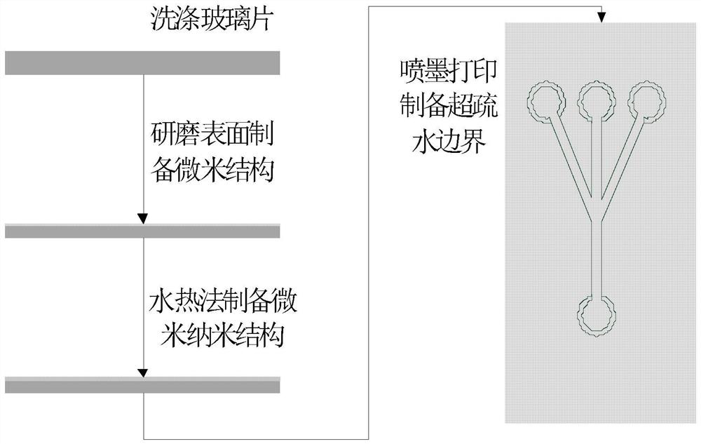
[0028] Specific implementation mode one: the following combination figure 1 Describe this embodiment, a method for manufacturing a planar microfluidic chip based on inkjet printing described in this embodiment, including:

[0029] Step 1. Clean the substrate and dry it;

[0030] Step 2. Grinding the substrate dried in step 1, and ultrasonic cleaning with deionized water after grinding;

[0031] Step 3, put one or more of deionized water, ammonia water, 0.1 to 5M sodium hydroxide solution and 0.1 to 5M potassium hydroxide solution in a closed container of polytetrafluoroethylene, and then ultrasonically clean the substrate In the airtight container of polytetrafluoroethylene, the substrate after ultrasonic cleaning is subjected to hydrothermal treatment for a time t, and then the substrate is taken out and dried at a constant temperature to obtain a substrate with a nano-rough structure; wherein, t is greater than or equal to 3 hours and less than or equal to 48 hours;

[003...


PUM

PropertyMeasurementUnit
particle size (mesh)aaaaaaaaaa

Abstract

The invention discloses a method for manufacturing a planar micro-fluidic chip based on ink-jet printing, and belongs to the fields of material surface treatment, microelectronic equipment and biochemical detection, and solves the problems of complex process, high cost and poor durability of the chip in the preparation process of the existing planar micro-fluidic chip. The method comprises the following steps: cleaning and drying a substrate; polishing the dried substrate and performing ultrasonic cleaning with deionized water; putting the ground substrate and one or more of deionized water, ammonia water, a 0.1-5M sodium hydroxide solution and a 0.1-5M potassium hydroxide solution into a polytetrafluoroethylene closed container for hydro-thermal treatment, taking out the substrate after time t, and drying the substrate at constant temperature to obtain a substrate with a nano coarse structure; preparing a super-hydrophobic pattern on the substrate through a micro-piezoelectric ink-jet printer; and after the substrate is printed, performing constant-temperature drying to obtain the planar micro-fluidic chip with the channel. The method is suitable for the technical field of material surface treatment.

Description

technical field [0001] The invention belongs to the fields of material surface treatment, microelectronic equipment and biochemical detection. Background technique [0002] In order to reduce the complexity of the equipment required for biochemical detection in the fields of medical treatment and environmental protection, and realize biochemical experiments anytime and anywhere, biochemical detection chips have become a research hotspot. The biochemical detection chip is the miniaturization, integration and automation of experimental equipment, which can concentrate the functions of sample preparation, separation and detection in the analysis laboratory on one chip. As an important branch of lab-on-a-chip, microfluidic chips based on microfluidic technology can make liquids react in micron-scale channels, and have the characteristics of less sample consumption, high throughput, fast speed, and no cross-contamination. [0003] Microfluidic chips are widely used and have been...

Claims


Application Information

Patent Timeline
Patent Type & Authority Applications(China)
IPC IPC(8): B01L3/00
CPCB01L3/502707
Inventor 陈亮姜舒月付强梁昊刘晓为张海峰曹伽牧
Owner HARBIN INST OF TECH
Why Eureka
Try Eureka