Light-emitting and light-filtering integrated optoelectronic chip and preparation method thereof

An optoelectronic chip and electrode technology, applied in the direction of optical filters, circuits, electrical components, etc., can solve problems such as complex optical path structure, achieve the effects of simplifying the optical path structure, improving accuracy and reliability, and wide application prospects

Pending Publication Date: 2022-04-15
NANJING UNIV OF POSTS & TELECOMM
View PDF0 Cites 0 Cited by
  • Summary
  • Abstract
  • Description
  • Claims
  • Application Information

AI Technical Summary

Problems solved by technology

[0004] The invention provides a light-emitting filter integrated optoelectronic chip and a preparation method thereof, which are used to solve the problem of complex optical path structure in the existing fluorescence analysis system and improve the accuracy of fluorescence analysis results

Method used


Image

  • Light-emitting and light-filtering integrated optoelectronic chip and preparation method thereof
  • Light-emitting and light-filtering integrated optoelectronic chip and preparation method thereof
  • Light-emitting and light-filtering integrated optoelectronic chip and preparation method thereof

Examples


Embodiment Construction

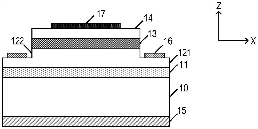
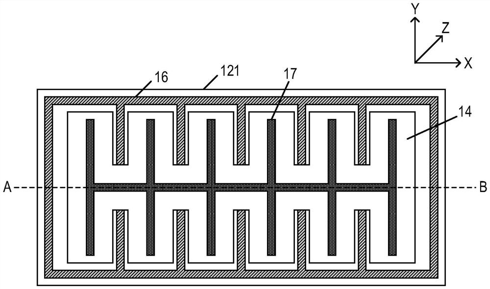
[0032] The specific implementation of the luminescence filter integrated optoelectronic chip and its preparation method provided by the present invention will be described in detail below with reference to the accompanying drawings.

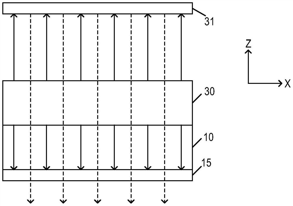
[0033] This specific embodiment provides a light-emitting filter integrated optoelectronic chip, with figure 1 It is a schematic cross-sectional view of the luminescent filter integrated optoelectronic chip in the specific embodiment of the present invention, and the attached figure 2 It is a schematic diagram of the three-dimensional structure of the light-emitting filter integrated optoelectronic chip in the specific embodiment of the present invention, and the attached image 3 It is a working principle diagram of the luminescent filter integrated optoelectronic chip in the specific embodiment of the present invention. figure 1 yes figure 2 A schematic cross-sectional view along the line AB, Figure 1-Figure 3 The X direction in is perpen...


PUM


Abstract

The invention relates to the technical field of semiconductors, in particular to a light-emitting and light-filtering integrated optoelectronic chip and a preparation method thereof. The light-emitting and light-filtering integrated optoelectronic chip comprises a transparent substrate which comprises a front surface and a back surface opposite to the front surface; the transparent LED device is located on the front face of the transparent substrate and comprises a buffer layer, an n-GaN layer, an InGaN / GaN quantum well layer and a p-GaN layer which are sequentially stacked in the direction perpendicular to the front face, and the transparent LED device at least can emit an emission light signal with a first wavelength in the direction from the back face to the front face; the light filtering device is located on the back face of the transparent substrate and used for transmitting an excitation fluorescence signal of a second wavelength and blocking the emission light signal, and the second wavelength is larger than the first wavelength. According to the invention, the light path structure in the fluorescence analysis process is simplified, and the accuracy and reliability of the fluorescence analysis result can be improved.

Description

technical field [0001] The invention relates to the technical field of semiconductors, in particular to a light-emitting filter integrated optoelectronic chip and a preparation method thereof. Background technique [0002] In the fields of biological sample detection and spectral analysis, when the detection light emitted by the light source irradiates the sample, the sample will excite long-wavelength fluorescence, and the relevant information of the sample will be loaded on the fluorescence. Afterwards, the excited fluorescence is collected by spectroscopic, optical filter and other devices for data analysis. Traditionally, fluorescence analysis requires a complex optical path system, such as integrating light source devices, spectroscopic devices, and optical filter devices, and adjusting the relative positional relationship between light source devices, spectroscopic devices, and optical filter devices, so as to realize functions such as fluorescence excitation and colle...

Claims


Application Information

Patent Timeline
IPC IPC(8): H01L33/48H01L33/00G02B5/20
CPCH01L33/483H01L33/007G02B5/20H01L2933/0033
Inventor 王永进宋永远高绪敏
Owner NANJING UNIV OF POSTS & TELECOMM
Why Eureka
Try Eureka