Check patentability & draft patents in minutes with Patsnap Eureka AI!

Output buffer for high and low voltage bus

An output buffer, high-voltage technology, applied in the input/output process of data processing, logic circuit coupling/interface using field effect transistors, instruments, etc., can solve problems such as the inability of integrated circuit chips to reach

Inactive Publication Date: 2006-02-08
INTEL CORP
View PDF2 Cites 0 Cited by
  • Summary
  • Abstract
  • Description
  • Claims
  • Application Information

AI Technical Summary

Problems solved by technology

In this state, IC chips cannot achieve modern performance levels as measured by speed, power, and / or both, for example, as long as the design uses only high-voltage-resistant transistors, although it will probably be compatible with conventional IC chips
IC chips, on the other hand, can operate at relatively low voltage levels and are therefore compatible with voltage levels of modern IC chips, but it is impossible to interface with conventional IC chips

Method used


Image

  • Output buffer for high and low voltage bus
  • Output buffer for high and low voltage bus
  • Output buffer for high and low voltage bus

Examples


Embodiment Construction

[0015] Numerous specific details are set forth in the following detailed description in order to provide a thorough understanding of the invention. However, it will be understood by those skilled in the art that the present invention may be practiced without these specific details. In other instances, well-known methods, processes, components and circuits have not been described in detail so as not to obscure the present invention.

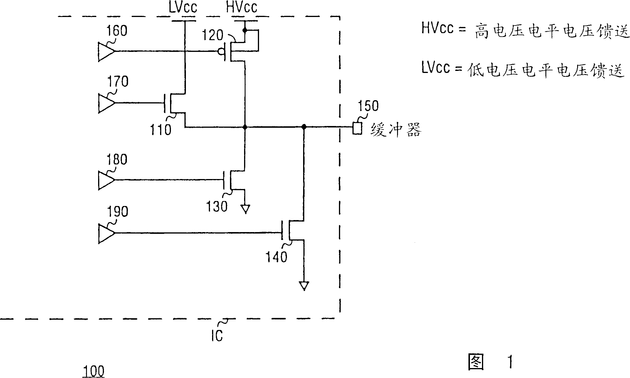
[0016] As first discussed the issues associated with designing and / or producing an integrated circuit chip are the input / output (I / O) voltage levels, or range of levels over which the integrated circuit chip is designed and operate as desired Work. As an example, and in no way intended to limit the scope of the invention, an integrated circuit chip may be designed to operate at input / output voltage levels ranging from about 1.8 volts to approximately 3.3 volts. In this case, at least not some form of fit. It is unlikely that such an integrated ...


PUM


Abstract

Briefly, in accordance with one embodiment of the invention, an integrated circuit includes: an output buffer. The output buffer includes semiconductor devices coupled to provide alternately activateable circuit configurations. The output buffer is adapted to couple to separate voltage supply voltage level ports and is further adapted to switch between the alternately activateable circuit configurations. The respective alternately activateable circuit configurations are respectively specifically adapted for interoperating with other integrated circuit chips, the respective threshold voltage levels of the semiconductor devices of different other integrated circuit chips being different. Briefly, in accordance with another embodiment of the invention, an output buffer includes: a plurality of thick gate metal-oxide semiconductor (MOS) transistors coupled in a circuit configuration. The plurality includes, as pull-up transistors, at least a thick gate P-channel MOS (PMOS) transistor and a thick gate N-channel MOS (NMOS) transistor, both respectively being coupled between separate voltage supply voltage level ports and an output port of the output buffer. The plurality further includes, as pull-down transistors, at least two more thick gate NMOS transistors, both respectively being coupled between ground and the output port. At least one of the pull-up transistors and one of the pull-down transistors is coupled in the circuit configuration to be driven on hard and to deliver a high voltage swing. Furthermore, at least one of the pull-up transistors and one of the pull-down transistors is coupled in the circuit configuration to be driven on less hard and to deliver a reduced voltage swing.

Description

technical field [0001] This invention relates to an output buffer, and more particularly to an output buffer of one or both integrated circuit (IC) chips capable of connecting high and low voltage buses. Background technique [0002] Coupling integrated circuit chips or ICs together presents a problem that is electrically compatible. Typically, integrated circuit chips are designed to operate at specific input / output (I / O) levels or substantially within level-specific constraints. However, with technical advantages, the level at which integrated circuit chips operate, including for I / O, has generally been reduced. Unfortunately, the trend to reduce voltage is much faster for core logic circuits, such as logic circuits that do not interface circuits outside of the chip, than for I / O, such as circuits that originally interface between chips. So current ICs typically support I / O levels that are higher than core logic levels. This allows improved performance of cores independ...

Claims


Application Information

Patent Timeline
Patent Type & Authority Patents(China)
IPC IPC(8): H03K19/0185G06F3/00H03K19/0175
CPCH03K19/018585H03K19/0185
Inventor L·T·克拉克T·J·莫兹德曾
Owner INTEL CORP
Features
  • R&D
  • Intellectual Property
  • Life Sciences
  • Materials
  • Tech Scout
  • Unparalleled Data Quality
  • Higher Quality Content
  • 60% Fewer Hallucinations
Learn More