

Laminating method and laminating device
A technology for bonding devices and bonding surfaces, applied in lamination devices, chemical instruments and methods, lamination auxiliary operations, etc., can solve problems such as difficulties in bonding foils, and achieve reliable bonding effects
- Summary
- Abstract
- Description
- Claims
- Application Information
AI Technical Summary
Problems solved by technology
Method used
Image

Examples
Embodiment Construction
[0027] Hereinafter, embodiments of the present invention will be described with reference to the drawings.
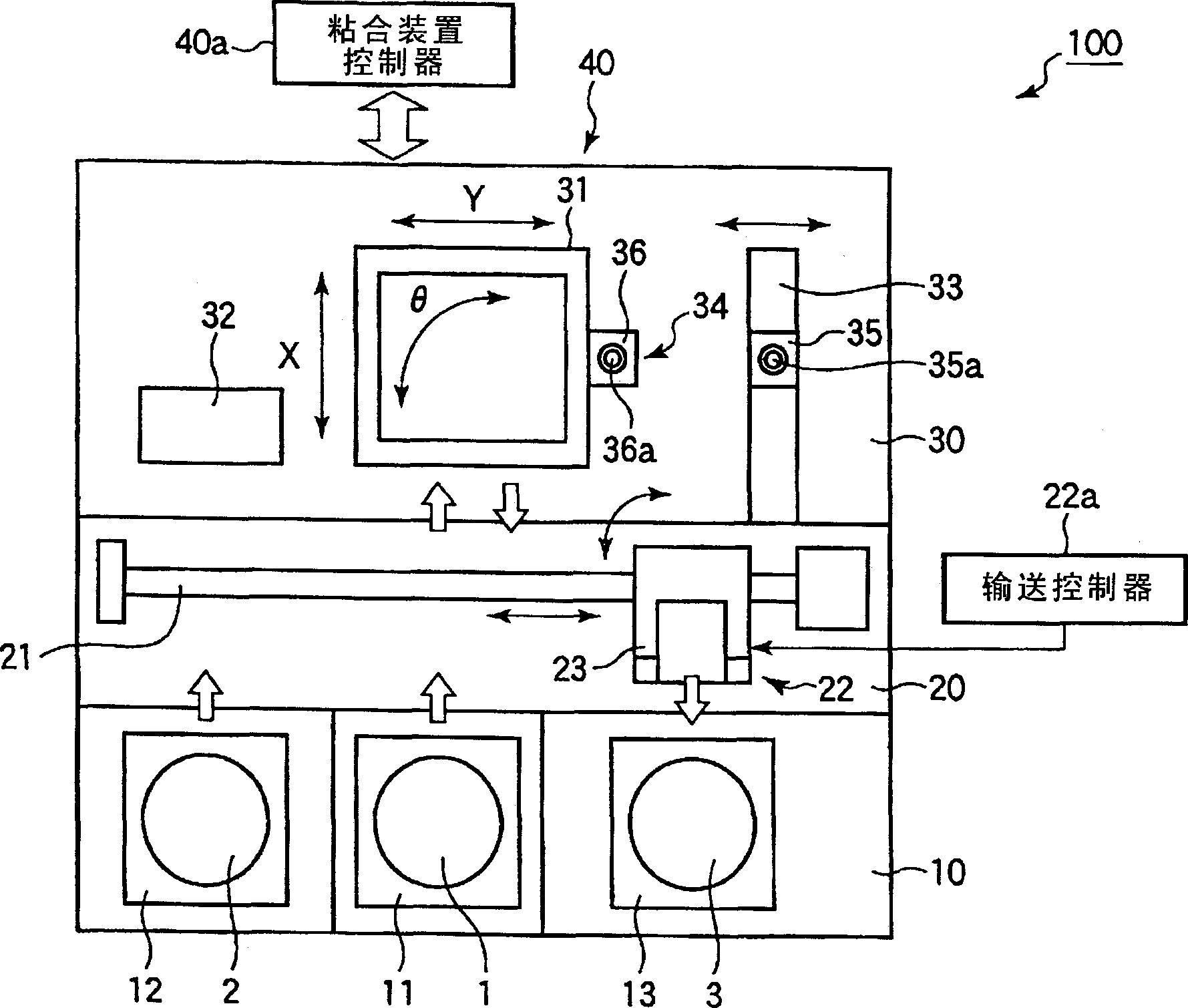
[0028] figure 1 is a schematic diagram of an example of the overall structure of a bonding system equipped with a bonding device according to an embodiment of the present invention. This bonding system 100 includes: a loading / unloading unit 10 for loading and unloading a thin plate body 1 to be bonded and a carrier 2 for transporting the thin plate body 1; Combining mechanism part 30, and conveying mechanism part 20 between them.
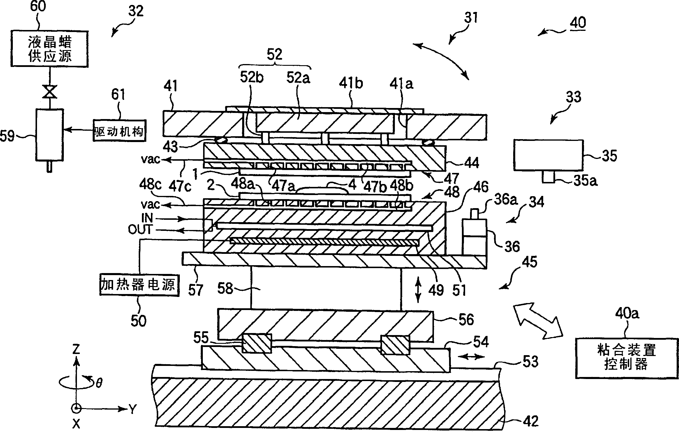
[0029] The bonding mechanism part 30 is provided with a bonding device 40 . This bonding device 40 has an apparatus main body 31 disposed in the center, and a liquid crystal wax supply mechanism 32 disposed on the side of the apparatus main body 31 for supplying liquid crystal wax to the carrier 2 in transit. In addition, reference numerals 33 and 34 in the illustration denote an upper side positioning mechanism and a lower side positionin...
PUM
| Property | Measurement | Unit |
|---|---|---|
| thickness | aaaaa | aaaaa |
Abstract
Description
Claims
Application Information