Semiconductor wafer mounting method and semiconductor wafer mounting apparatus

A film sticking device and semiconductor technology, which is applied in the fields of semiconductor devices, semiconductor/solid-state device manufacturing, electric solid-state devices, etc., can solve problems such as wafer breakage, and achieve the effect of suppressing poor electrical connection.

Inactive Publication Date: 2014-05-07
NITTO DENKO CORP
View PDF4 Cites 12 Cited by
  • Summary
  • Abstract
  • Description
  • Claims
  • Application Information

AI Technical Summary

Problems solved by technology

In other words, a new problem arises that the edge of the wafer is damaged due to the influence of the tensile force.

Method used


Image

  • Semiconductor wafer mounting method and semiconductor wafer mounting apparatus
  • Semiconductor wafer mounting method and semiconductor wafer mounting apparatus
  • Semiconductor wafer mounting method and semiconductor wafer mounting apparatus

Examples


Embodiment Construction

[0057] Hereinafter, embodiments of the present invention will be described with reference to the drawings.

[0058] semiconductor wafer

[0059] In this embodiment, a semiconductor wafer (hereinafter, simply referred to as a “wafer”) adhered and held by a ring frame with an adhesive tape (dicing tape) for support will be described in detail.

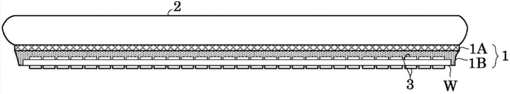
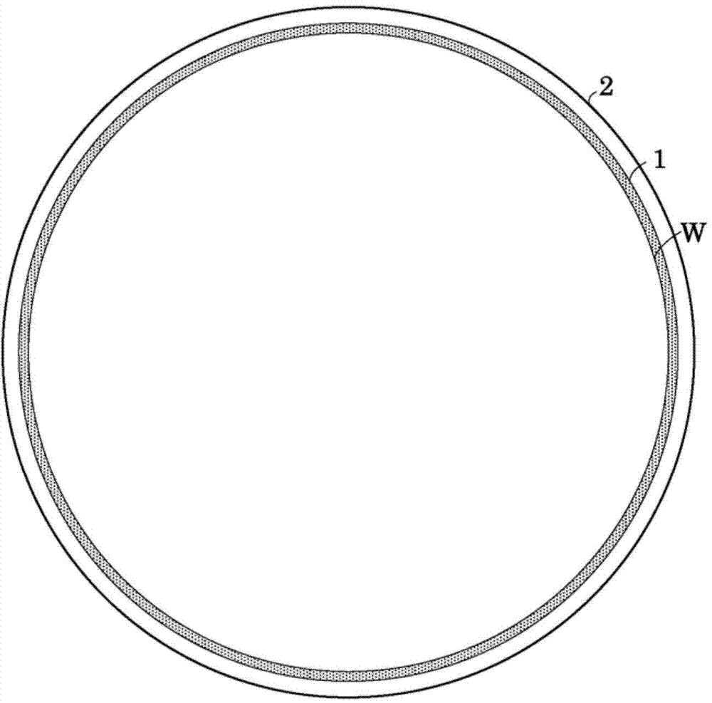
[0060] figure 1 shows a longitudinal sectional view of a semiconductor wafer of the present invention, figure 2 A bottom view of the semiconductor wafer is shown.

[0061] The wafer W is bonded with a support plate 2 for reinforcement by means of a plurality of adhesive layers 1 . Protruding electrodes 3 such as solder balls and bumps are formed on the back surface and the front surface of the wafer W after back grinding. For example, the thickness of the wafer W is 100 μm or less, the thickness of the protruding electrodes 3 and the distance between the protruding electrodes are 100 μm.

[0062] The adhesive layer 1 is composed ...


PUM


Abstract

The invention provides a semiconductor wafer mounting method and a semiconductor wafer mounting apparatus. A resin sealing sheet is cut into an adhesive sheet piece having an outer shape smaller than that of a wafer. The adhesive sheet piece is joined to a supporting adhesive tape together with a ring frame. The adhesive tape between the ring frame and the adhesive sheet piece is sandwiched by upper and lower housings to form a chamber. The wafer with a support board placed on a wafer holding table within the chamber faces to the adhesive sheet piece closely. The chamber is divided into two spaces by the adhesive tape. Differential pressure generated within the two spaces causes the adhesive tape and the adhesive sheet piece to cave and bend toward the wafer, whereby the adhesive sheet piece is joined to the wafer.

Description

technical field [0001] The present invention relates to a method for attaching a semiconductor wafer to a ring frame by means of an adhesive tape for support, and a film attaching device for the semiconductor wafer, and more particularly relates to a sheet for connection reinforcement interposed between the adhesive tape and protrusions formed on the back side The technology of attaching the semiconductor wafer to the adhesive tape by means of electrodes between the semiconductor wafers. Background technique [0002] A general semiconductor device has protruding electrodes formed on its main surface (back surface) to be mounted on a wiring substrate. The protruding electrodes are formed of, for example, solder balls, bumps, or the like. [0003] When mounting a semiconductor device on an electrode of a wiring board, an underfill sheet is attached to a wafer as a sheet for bonding the semiconductor device to a mounting position of the wiring board. Thereafter, the singulate...

Claims


Application Information

Patent Timeline
Patent Type & Authority Applications(China)
IPC IPC(8): H01L21/02H01L21/67
CPCH01L21/67132H01L21/6835H01L21/6836H01L2221/68318H01L2221/68327H01L2221/68381H01L2924/13055H01L2924/00H01L2924/1305H01L2924/1461H01L21/30H01L21/683
Inventor 山本雅之金岛安治石井直树
Owner NITTO DENKO CORP
Why Eureka
Try Eureka